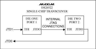
Abstract: This application note describes the JTAG hardware boundary scan functions of the quad port single chip transceivers (SCTs). The JTAG functionality for the quad port devices is essentially the same as four separate DS21x5y devices daisy chained together. The DS21Q352, DS21Q354, DS21Q552, DS21Q554, and DS21Q55 do not have a single BSDL file because they are multichip modules that contain four separate die in the same package. The internal JTAG pins are either wired together in parallel or daisy chained as appropriate. The JTDI pin is connected to the JTDI input of the first die, while JTDO4 pin is connected to the JTDO output of the fourth die. JTRST, JTCLK, and JTMS are wired together in parallel. To complete the scan chain, four copies of the specific DS21x5y BSDL file need to be placed in the JTAG chain. The note contains a complete breakdown of the JTAG scan chain and explains how to access all of the boundary scan cells in the device.
To alleviate the need for mapping individual pins on the BGA substrate the following Table 1 has been provided. The table contains the port location (SCT number), BGA pin, BSDL cell scan position, BSDL cell name, and other useful information. The table has been sorted by port location (SCT number) and then BSDL scan position. This should allow for easy access to the necessary information about which BSDL scan position maps to which port location and BGA pin number.
The BSDL files for the various DS21x5y devices can be found on the web at: BSDL Files.
Table 1. JTAG scan chain: BGA pin to BSDL cell mapping
Introduction
The JTAG functionality for the DS21Qx5y devices is essentially the same as four separate DS21x5y devices daisy chained together. The DS21Q352, DS21Q354, DS21Q552, and DS21Q554 do not have a single BSDL file because they are multichip modules that contain four separate die in the same package, with some of the pins wired together internally. The internal JTAG pins are either wired together in parallel or daisy chained as appropriate. The JTDI pin is connected to the JTDI input of the first die, while JTDO4 pin is connected to the JTDO output of the fourth die. JTRST, JTCLK, and JTMS are simply wired together in parallel. Because of this, four copies of the specific DS21x5y device BSDL file need to be placed in the JTAG chain for scanning the internal daisy chain of the DS21Qx5y.Recommendation for JTAG Design
In most cases, the DS21Qx5y device symbol was created as a single entity. In reality, the base of the DS21Qx5y is simply a printed wire board with the DS21x5y die with the connections detailed in the DS21Qx5y data sheet. To solve this issue, some additional work may be required to reflect the fact that the device is actually made up of four separate die. If the DS21Qx5y device and associated BSDL files are being used in a simulation program, there are two possible solutions. The easiest way to solve this problem is to alter the netlist after the design is complete to account for the internal connections. Another way is to create a hierarchy in the design. It is fairly simple to layout an extra page or two of schematic to reflect these internal connections. If however there is no need for the simulation and the DS21Qx5y is only being run on a physical board, the BSDL files can simply be used as is.To alleviate the need for mapping individual pins on the BGA substrate the following Table 1 has been provided. The table contains the port location (SCT number), BGA pin, BSDL cell scan position, BSDL cell name, and other useful information. The table has been sorted by port location (SCT number) and then BSDL scan position. This should allow for easy access to the necessary information about which BSDL scan position maps to which port location and BGA pin number.
The BSDL files for the various DS21x5y devices can be found on the web at: BSDL Files.
Table 1. JTAG scan chain: BGA pin to BSDL cell mapping
| SCT PORT |
BGA PIN | BSDL SCAN POSITION |
BSDL SCAN NAME |
I/O | DATA SHEET SYMBOL |
DATA SHEET DESCRIPTION |
| 1 | -- | 0 | RCL | Output | -- | Internal to Package |
| 1 | M1 | 1 | A8MCLK | Output | 8MCLK1 | 8192 MHz Clock Based on RCLK1 |
| 1 | M2 | 2 | RCHBLK | Output | RCHBLK1 | Receive Channel Block SCT1 |
| 1 | H1 | 3 | RSYSCLK | Input | RSYSCLK1 | Receive System Clock SCT1 |
| 1 | H2 | 4 | RLOSLOTC | Output | RLOS/LOTC1 | Receive LOS/LOTC SCT1 |
| 1 | G1 | 5 | RSYNC | BiDir | RSYNC1 | Receive Sync SCT1 |
| 1 | -- | 6 | -- | Control | -- | Internal to Package |
| 1 | K4 | 7 | RFSYNC | Output | RFSYNC1 | Receive Frame Sync SCT1 |
| 1 | L1 | 8 | RMSYNC | Output | RMSYNC1 | Receive Multiframe Sync SCT1 |
| 1 | J2 | 9 | RSER | Output | RSER1 | Receive Serial Data SCT1 |
| 1 | L2 | 10 | RSIG | Output | RSIG1 | Receive Signaling Output SCT1 |
| 1 | K1 | 11 | RSIGF | Output | RSIGF1 | Receive Signaling Freeze SCT1 |
| 1 | J1 | 12 | RCHCLK | Output | RCHCLK1 | Receive Channel Clock SCT1 |
| 1 | L4 | 13 | RPOSO | Output | RPOSO1 | Receive Positive Data Output SCT1 |
| 1 | L3 | 14 | RNEGO | Output | RNEGO1 | Receive Negative Data Output SCT1 |
| 1 | M3 | 15 | RCLKO | Output | RCLKO1 | Receive Clock Output SCT1 |
| 1 | M4 | 16 | RCLKI | Input | RCLKI1 | Receive Clock Input SCT1 |
| 1 | R3 | 17 | RNEGI | Input | RNEGI1 | Receive Negative Data Input SCT1 |
| 1 | R4 | 18 | RPOSI | Input | RPOSI1 | Receive Positive Data Input SCT1 |
| 1 | -- | 19 | RDATA | Output | -- | Internal to Package |
| 1 | N3 | 20 | RCLK | Output | RCLK1 | Receive Clock SCT1 |
| 1 | F1 | 21 | RLCLK | Output | RLCLK1 | Receive Link Clock SCT1 |
| 1 | G2 | 22 | RLINK | Output | RLINK1 | Receive Link Data SCT1 |
| 1 | K3 | 23 | WRRW | Input | Active-Low WR (R/Active-Low W) | Write Input (Read/Write) |
| 1 | -- | 24 | FMS | Input | -- | Internal to Package |
| 1 | P3 | 25 | CS | Input | Active-Low CS1 | Chip Select SCT1 |
| 1 | N2 | 26 | RDDS | Input | Active-Low RD (Active-Low DS) | Read Input (Data Strobe) |
| 1 | P4 | 27 | ALEASA7 | Input | A7/ALE | Address Bus Bit 7/ALE |
| 1 | U8 | 28 | A6 | Input | A6 | Address Bus Bit 6 |
| 1 | H4 | 29 | A5 | Input | A5 | Address Bus Bit 5 |
| 1 | V8 | 30 | A4 | Input | A4 | Address Bus Bit 4 |
| 1 | T4 | 31 | A3 | Input | A3 | Address Bus Bit 3 |
| 1 | V2 | 32 | A2 | Input | A2 | Address Bus Bit 2 |
| 1 | L17 | 33 | A1 | Input | A1 | Address Bus Bit 1 |
| 1 | U3 | 34 | A0 | Input | A0 | Address Bus Bit 0 |
| 1 | U4 | 35 | D7AD7 | BiDir | D7/AD7 | Data or Address/Data Bus Bit 7 |
| 1 | V4 | 36 | D6AD6 | BiDir | D6/AD6 | Data or Address/Data Bus Bit 6 |
| 1 | U5 | 37 | D5AD5 | BiDir | D5/AD5 | Data or Address/Data Bus Bit 5 |
| 1 | U9 | 38 | D4AD4 | BiDir | D4/AD4 | Data or Address/Data Bus Bit 4 |
| 1 | U7 | 39 | D3AD3 | BiDir | D3/AD3 | Data or Address/Data Bus Bit 3 |
| 1 | W15 | 40 | D2AD2 | BiDir | D2/AD2 | Data or Address/Data Bus Bit 2 |
| 1 | J19 | 41 | D1AD1 | BiDir | D1/AD1 | Data or Address/Data Bus Bit 1 |
| 1 | U11 | 42 | D0AD0 | BiDir | D0/AD0 | Data or Address/Data Bus Bit 0 |
| 1 | -- | 43 | -- | Control | -- | Internal to Package |
| 1 | U10 | 44 | MUX | Input | MUX | Mux Bus Select |
| 1 | V9 | 45 | CO | Output | CO1 | Carry Output for IBO SCT1 |
| 1 | V10 | 46 | TCHCLK | Output | TCHCLK1 | Transmit Channel Clock SCT1 |
| 1 | W12 | 47 | TSSYNC | Input | TSSYNC1 | Transmit System Sync SCT1 |
| 1 | W11 | 48 | TSYSCLK | Input | TSYSCLK1 | Transmit System Clock SCT1 |
| 1 | -- | 49 | TDATA | Input | -- | Internal to Package |
| 1 | -- | 50 | TESO | Output | -- | Internal to Package |
| 1 | W10 | 51 | TSIG | Input | TSIG1 | Transmit Signaling Input SCT1 |
| 1 | W9 | 52 | TSER | Input | TSER1 | Transmit Serial Data SCT1 |
| 1 | Y9 | 53 | TCLK | Input | TCLK1 | Transmit Clock SCT1 |
| 1 | V7 | 54 | TPOSO | Output | TPOSO1 | Transmit Positive Data Output SCT1 |
| 1 | T3 | 55 | TNEGO | Output | TNEGO1 | Transmit Negative Data Output SCT1 |
| 1 | W7 | 56 | TCLKO | Output | TCLKO1 | Transmit Clock Output SCT1 |
| 1 | V6 | 57 | TCLKI | Input | TCLKI1 | Transmit Clock Input SCT1 |
| 1 | R1 | 58 | TNEGI | Input | TNEGI1 | Transmit Negative Data Input SCT1 |
| 1 | W3 | 59 | TPOSI | Input | TPOSI1 | Transmit Positive Data Input SCT1 |
| 1 | V1 | 60 | TSYNC | BiDir | TSYNC1 | Transmit Sync SCT1 |
| 1 | -- | 61 | -- | Control | -- | Internal to Package |
| 1 | W6 | 62 | CI | Input | CI1 | Carry Input for IBO SCT1 |
| 1 | W5 | 63 | TLINK | Input | TLINK1 | Transmit Link Data for SCT1 |
| 1 | V3 | 64 | TLCLK | Output | TLCLK1 | Transmit Link Clock for SCT1 |
| 1 | W1 | 65 | TCHBLK | Output | TCHBLK1 | Transmit Channel Block SCT1 |
| 1 | U1 | 66 | INT | Output | Active-Low INT | Interrupt |
| 1 | -- | 67 | -- | Internal | -- | Internal to Package |
| 1 | -- | 68 | -- | Internal | -- | Internal to Package |
| 1 | U16 | 69 | TEST | Input | TEST | Test |
| 1 | -- | 70 | A8XCLK | Output | -- | Internal to Package |
| 1 | K2 | 71 | LIUC | Input | LIUC | Line Interface Connect |
| 1 | P2 | 72 | BTS | Input | BTS | Bus Type Select |
| 2 | -- | 0 | RCL | Output | -- | Internal to Package |
| 2 | H17 | 1 | A8MCLK | Output | 8MCLK2 | 8192MHz Clock Based on RCLK2 |
| 2 | G17 | 2 | RCHBLK | Output | RCHBLK2 | Receive Channel Block SCT2 |
| 2 | F17 | 3 | RSYSCLK | Input | RSYSCLK2 | Receive System Clock SCT2 |
| 2 | E17 | 4 | RLOSLOTC | Output | RLOS/LOTC2 | Receive LOS/LOTC SCT2 |
| 2 | D12 | 5 | RSYNC | BiDir | RSYNC2 | Receive Sync SCT2 |
| 2 | -- | 6 | -- | Control | -- | Internal to Package |
| 2 | D17 | 7 | RFSYNC | Output | RFSYNC2 | Receive Frame Sync SCT2 |
| 2 | D16 | 8 | RMSYNC | Output | RMSYNC2 | Receive Multiframe Sync SCT2 |
| 2 | D15 | 9 | RSER | Output | RSER2 | Receive Serial Data SCT2 |
| 2 | B16 | 10 | RSIG | Output | RSIG2 | Receive Signaling Output SCT2 |
| 2 | C15 | 11 | RSIGF | Output | RSIGF2 | Receive Signaling Freeze SCT2 |
| 2 | D14 | 12 | RCHCLK | Output | RCHCLK2 | Receive Channel Clock SCT2 |
| 2 | A16 | 13 | RPOSO | Output | RPOSO2 | Receive Positive Data Output SCT2 |
| 2 | B15 | 14 | RNEGO | Output | RNEGO2 | Receive Negative Data Output SCT2 |
| 2 | C14 | 15 | RCLKO | Output | RCLKO2 | Receive Clock Output SCT2 |
| 2 | A15 | 16 | RCLKI | Input | RCLKI2 | Receive Clock Input SCT2 |
| 2 | D13 | 17 | RNEGI | Input | RNEGI2 | Receive Negative Data Input SCT2 |
| 2 | B14 | 18 | RPOSI | Input | RPOSI2 | Receive Positive Data Input SCT2 |
| 2 | -- | 19 | RDATA | Output | -- | Internal to Package |
| 2 | B13 | 20 | RCLK | Output | RCLK2 | Receive Clock SCT2 |
| 2 | A12 | 21 | RLCLK | Output | RLCLK2 | Receive Link Clock SCT2 |
| 2 | A13 | 22 | RLINK | Output | RLINK2 | Receive Link Data SCT2 |
| 2 | K3 | 23 | WRRW | Input | Active-Low WR (R/Active-Low W) | Write Input (Read/Write) |
| 2 | -- | 24 | FMS | Input | -- | Internal to Package |
| 2 | A14 | 25 | CS | Input | Active-Low CS2 | Chip Select for SCT2 |
| 2 | N2 | 26 | RDDS | Input | Active-Low RD (Active-Low DS) | Read Input (Data Strobe) |
| 2 | P4 | 27 | ALEASA7 | Input | A7/ALE | Address Bus Bit 7/ALE |
| 2 | U8 | 28 | A6 | Input | A6 | Address Bus Bit 6 |
| 2 | H4 | 29 | A5 | Input | A5 | Address Bus Bit 5 |
| 2 | V8 | 30 | A4 | Input | A4 | Address Bus Bit 4 |
| 2 | T4 | 31 | A3 | Input | A3 | Address Bus Bit 3 |
| 2 | V2 | 32 | A2 | Input | A2 | Address Bus Bit 2 |
| 2 | L17 | 33 | A1 | Input | A1 | Address Bus Bit 1 |
| 2 | U3 | 34 | A0 | Input | A0 | Address Bus Bit 0 |
| 2 | U4 | 35 | D7AD7 | BiDir | D7/AD7 | Data or Address/Data Bus Bit 7 |
| 2 | V4 | 36 | D6AD6 | BiDir | D6/AD6 | Data or Address/Data Bus Bit 6 |
| 2 | U5 | 37 | D5AD5 | BiDir | D5/AD5 | Data or Address/Data Bus Bit 5 |
| 2 | U9 | 38 | D4AD4 | BiDir | D4/AD4 | Data or Address/Data Bus Bit 4 |
| 2 | U7 | 39 | D3AD3 | BiDir | D3/AD3 | Data or Address/Data Bus Bit 3 |
| 2 | W15 | 40 | D2AD2 | BiDir | D2/AD2 | Data or Address/Data Bus Bit 2 |
| 2 | J19 | 41 | D1AD1 | BiDir | D1/AD1 | Data or Address/Data Bus Bit 1 |
| 2 | U11 | 42 | D0AD0 | BiDir | D0/AD0 | Data or Address/Data Bus Bit 0 |
| 2 | -- | 43 | -- | Control | -- | Internal to Package |
| 2 | U10 | 44 | MUX | Input | MUX | Mux Bus Select |
| 2 | B17 | 45 | CO | Output | CO2 | Carry Output for IBO SCT2 |
| 2 | A18 | 46 | TCHCLK | Output | TCHCLK2 | Transmit Channel Clock SCT2 |
| 2 | B18 | 47 | TSSYNC | Input | TSSYNC2 | Transmit System Sync SCT2 |
| 2 | A19 | 48 | TSYSCLK | Input | TSYSCLK2 | Transmit System Clock SCT2 |
| 2 | -- | 49 | TDATA | Input | -- | Internal to Package |
| 2 | -- | 50 | TESO | Output | -- | Internal to Package |
| 2 | C18 | 51 | TSIG | Input | TSIG2 | Transmit Signaling Input SCT2 |
| 2 | C17 | 52 | TSER | Input | TSER2 | Transmit Serial Data SCT2 |
| 2 | B19 | 53 | TCLK | Input | TCLK2 | Transmit Clock SCT2 |
| 2 | C19 | 54 | TPOSO | Output | TPOSO2 | Transmit Positive Data Output SCT2 |
| 2 | B20 | 55 | TNEGO | Output | TNEGO2 | Transmit Negative Data Output SCT2 |
| 2 | E18 | 56 | TCLKO | Output | TCLKO2 | Transmit Clock Output SCT2 |
| 2 | D19 | 57 | TCLKI | Input | TCLKI2 | Transmit Clock Input SCT2 |
| 2 | F19 | 58 | TNEGI | Input | TNEGI2 | Transmit Negative Data Input SCT2 |
| 2 | C20 | 59 | TPOSI | Input | TPOSI2 | Transmit Positive Data Intput SCT2 |
| 2 | D20 | 60 | TSYNC | BiDir | TSYNC2 | Transmit Sync SCT2 |
| 2 | -- | 61 | -- | Control | -- | Internal to Package |
| 2 | F18 | 62 | CI | Input | CI2 | Carry Input for IBO SCT2 |
| 2 | E19 | 63 | TLINK | Input | TLINK2 | Transmit Link Data for SCT2 |
| 2 | E20 | 64 | TLCLK | Output | TLCLK2 | Transmit Link Clock for SCT2 |
| 2 | F20 | 65 | TCHBLK | Output | TCHBLK2 | Transmit Channel Block SCT2 |
| 2 | U1 | 66 | INT | Output | Active-Low INT | Interrupt |
| 2 | -- | 67 | -- | Internal | -- | Internal to Package |
| 2 | -- | 68 | -- | Internal | -- | Internal to Package |
| 2 | U16 | 69 | TEST | Input | TEST | Test |
| 2 | -- | 70 | A8XCLK | Output | -- | Internal to Package |
| 2 | K2 | 71 | LIUC | Input | LIUC | Line Interface Connect |
| 2 | P2 | 72 | BTS | Input | BTS | Bus Type Select |
| 3 | -- | 0 | RCL | Output | -- | Internal to Package |
| 3 | F4 | 1 | A8MCLK | Output | 8MCLK3 | 8192 MHz Clock Based on RCLK3 |
| 3 | G4 | 2 | RCHBLK | Output | RCHBLK3 | Receive Channel Block SCT3 |
| 3 | G3 | 3 | RSYSCLK | Input | RSYSCLK3 | Receive System Clock SCT3 |
| 3 | E1 | 4 | RLOSLOTC | Output | RLOS/LOTC3 | Receive LOS/LOTC SCT3 |
| 3 | D1 | 5 | RSYNC | BiDir | RSYNC3 | Receive Sync SCT3 |
| 3 | -- | 6 | -- | Control | -- | Internal to Package |
| 3 | A2 | 7 | RFSYNC | Output | RFSYNC3 | Receive Frame Sync SCT3 |
| 3 | F2 | 8 | RMSYNC | Output | RMSYNC3 | Receive Multiframe Sync SCT3 |
| 3 | E2 | 9 | RSER | Output | RSER3 | Receive Serial Data SCT3 |
| 3 | C1 | 10 | RSIG | Output | RSIG3 | Receive Signaling Output SCT3 |
| 3 | D2 | 11 | RSIGF | Output | RSIGF3 | Receive Signaling Freeze SCT3 |
| 3 | F3 | 12 | RCHCLK | Output | RCHCLK3 | Receive Channel Clock SCT3 |
| 3 | B1 | 13 | RPOSO | Output | RPOSO3 | Receive Positive Data Output SCT3 |
| 3 | C2 | 14 | RNEGO | Output | RNEGO3 | Receive Negative Data Output SCT3 |
| 3 | B4 | 15 | RCLKO | Output | RCLKO3 | Receive Clock Output SCT3 |
| 3 | A4 | 16 | RCLKI | Input | RCLKI3 | Receive Clock Input SCT3 |
| 3 | A1 | 17 | RNEGI | Input | RNEGI3 | Receive Negative Data Input SCT3 |
| 3 | B2 | 18 | RPOSI | Input | RPOSI3 | Receive Positive Data Input SCT3 |
| 3 | -- | 19 | RDATA | Output | -- | Internal to Package |
| 3 | E3 | 20 | RCLK | Output | RCLK3 | Receive Clock SCT3 |
| 3 | D3 | 21 | RLCLK | Output | RLCLK3 | Receive Link Clock SCT3 |
| 3 | A3 | 22 | RLINK | Output | RLINK3 | Receive Link Data SCT3 |
| 3 | K3 | 23 | WRRW | Input | Active-Low WR (R/Active-Low W) | Write Input (Read/Write) |
| 3 | -- | 24 | FMS | Input | -- | Internal to Package |
| 3 | B5 | 25 | CS | Input | Active-Low CS3 | Chip Select for SCT3 |
| 3 | N2 | 26 | RDDS | Input | Active-Low RD (Active-Low DS) | Read Input (Data Strobe) |
| 3 | P4 | 27 | ALEASA7 | Input | A7/ALE | Address Bus Bit 7/ALE |
| 3 | U8 | 28 | A6 | Input | A6 | Address Bus Bit 6 |
| 3 | H4 | 29 | A5 | Input | A5 | Address Bus Bit 5 |
| 3 | V8 | 30 | A4 | Input | A4 | Address Bus Bit 4 |
| 3 | T4 | 31 | A3 | Input | A3 | Address Bus Bit 3 |
| 3 | V2 | 32 | A2 | Input | A2 | Address Bus Bit 2 |
| 3 | L17 | 33 | A1 | Input | A1 | Address Bus Bit 1 |
| 3 | U3 | 34 | A0 | Input | A0 | Address Bus Bit 0 |
| 3 | U4 | 35 | D7AD7 | BiDir | D7/AD7 | Data or Address/Data Bus Bit 7 |
| 3 | V4 | 36 | D6AD6 | BiDir | D6/AD6 | Data or Address/Data Bus Bit 6 |
| 3 | U5 | 37 | D5AD5 | BiDir | D5/AD5 | Data or Address/Data Bus Bit 5 |
| 3 | U9 | 38 | D4AD4 | BiDir | D4/AD4 | Data or Address/Data Bus Bit 4 |
| 3 | U7 | 39 | D3AD3 | BiDir | D3/AD3 | Data or Address/Data Bus Bit 3 |
| 3 | W15 | 40 | D2AD2 | BiDir | D2/AD2 | Data or Address/Data Bus Bit 2 |
| 3 | J19 | 41 | D1AD1 | BiDir | D1/AD1 | Data or Address/Data Bus Bit 1 |
| 3 | U11 | 42 | D0AD0 | BiDir | D0/AD0 | Data or Address/Data Bus Bit 0 |
| 3 | -- | 43 | -- | Control | -- | Internal to Package |
| 3 | U10 | 44 | MUX | Input | MUX | Mux Bus Select |
| 3 | A6 | 45 | CO | Output | CO3 | Carry Output for IBO SCT3 |
| 3 | B8 | 46 | TCHCLK | Output | TCHCLK3 | Transmit Channel Clock SCT3 |
| 3 | D10 | 47 | TSSYNC | Input | TSSYNC3 | Transmit System Sync SCT3 |
| 3 | A11 | 48 | TSYSCLK | Input | TSYSCLK3 | Transmit System Clock SCT3 |
| 3 | -- | 49 | TDATA | Input | -- | Internal to Package |
| 3 | -- | 50 | TESO | Output | -- | Internal to Package |
| 3 | A10 | 51 | TSIG | Input | TSIG3 | Transmit Signaling Input SCT3 |
| 3 | C10 | 52 | TSER | Input | TSER3 | Transmit Serial Data SCT3 |
| 3 | B10 | 53 | TCLK | Input | TCLK3 | Transmit Clock SCT3 |
| 3 | C9 | 54 | TPOSO | Output | TPOSO3 | Transmit Positive Data Output SCT3 |
| 3 | D9 | 55 | TNEGO | Output | TNEGO3 | Transmit Negative Data Output SCT3 |
| 3 | A7 | 56 | TCLKO | Output | TCLKO3 | Transmit Clock Output SCT3 |
| 3 | C8 | 57 | TCLKI | Input | TCLKI3 | Transmit Clock Input SCT3 |
| 3 | D8 | 58 | TNEGI | Input | TNEGI3 | Transmit Negative Data Input SCT3 |
| 3 | A8 | 59 | TPOSI | Input | TPOSI3 | Transmit Positive Data Input SCT3 |
| 3 | C7 | 60 | TSYNC | BiDir | TSYNC3 | Transmit Sync SCT3 |
| 3 | -- | 61 | -- | Control | -- | Internal to Package |
| 3 | D7 | 62 | CI | Intput | CI3 | Carry Input for IBO SCT3 |
| 3 | C6 | 63 | TLINK | Input | TLINK3 | Transmit Link Data for SCT3 |
| 3 | D6 | 64 | TLCLK | Output | TLCLK3 | Transmit Link Clock for SCT3 |
| 3 | C11 | 65 | TCHBLK | Output | TCHBLK3 | Transmit Channel Block SCT3 |
| 3 | U1 | 66 | INT | Output | Active-Low INT | Interrupt for All Four SCTs |
| 3 | -- | 67 | -- | Internal | -- | Internal to Package |
| 3 | -- | 68 | -- | Internal | -- | Internal to Package |
| 3 | U16 | 69 | TEST | Input | TEST | Test |
| 3 | -- | 70 | A8XCLK | Output | -- | Internal to Package |
| 3 | K2 | 71 | LIUC | Input | LIUC | Line Interface Connect |
| 3 | P2 | 72 | BTS | Input | BTS | Bus Type Select |
| 4 | -- | 0 | RCL | Output | -- | Internal to Package |
| 4 | V13 | 1 | A8MCLK | Output | 8MCLK4 | 8192MHz Clock Based on RCLK4 |
| 4 | Y12 | 2 | RCHBLK | Output | RCHBLK4 | Receive Channel Block SCT4 |
| 4 | W14 | 3 | RSYSCLK | Input | RSYSCLK4 | Receive System Clock SCT4 |
| 4 | V11 | 4 | RLOSLOTC | Output | RLOS/LOTC4 | Receive LOS/LOTC SCT4 |
| 4 | V12 | 5 | RSYNC | BiDir | RSYNC4 | Receive Sync SCT4 |
| 4 | -- | 6 | -- | Control | -- | Internal to Package |
| 4 | V14 | 7 | RFSYNC | Output | RFSYNC4 | Receive Frame Sync SCT4 |
| 4 | W16 | 8 | RMSYNC | Output | RMSYNC4 | Receive Multiframe Sync SCT4 |
| 4 | W17 | 9 | RSER | Output | RSER4 | Receive Serial Data SCT4 |
| 4 | Y18 | 10 | RSIG | Output | RSIG4 | Receive Signaling Output SCT4 |
| 4 | V16 | 11 | RSIGF | Output | RSIGF4 | Receive Signaling Freeze SCT4 |
| 4 | U14 | 12 | RCHCLK | Output | RCHCLK4 | Receive Channel Clock SCT4 |
| 4 | U15 | 13 | RPOSO | Output | RPOSO4 | Receive Positive Data Output SCT4 |
| 4 | U17 | 14 | RNEGO | Output | RNEGO4 | Receive Negative Data Output SCT4 |
| 4 | T17 | 15 | RCLKO | Output | RCLKO4 | Receive Clock Output SCT4 |
| 4 | R17 | 16 | RCLKI | Input | RCLKI4 | Receive Clock Input SCT4 |
| 4 | P17 | 17 | RNEGI | Input | RNEGI4 | Receive Negative Data Input SCT4 |
| 4 | V15 | 18 | RPOSI | Input | RPOSI4 | Receive Positive Data Input SCT4 |
| 4 | -- | 19 | RDATA | Output | -- | Internal to Package |
| 4 | M18 | 20 | RCLK | Output | RCLK4 | Receive Clock SCT4 |
| 4 | K18 | 21 | RLCLK | Output | RLCLK4 | Receive Link Clock SCT4 |
| 4 | U12 | 22 | RLINK | Output | RLINK4 | Receive Link Data SCT4 |
| 4 | K3 | 23 | WRRW | Input | Active-Low WR (R/Active-Low W) | Write Input (Read/Write) |
| 4 | -- | 24 | FMS | Input | -- | Internal to Package |
| 4 | K17 | 25 | CS | Input | Active-Low CS4 | Chip Select for SCT4 |
| 4 | N2 | 26 | RDDS | Input | Active-Low RD (Active-Low DS) | Read Input (Data Strobe) |
| 4 | P4 | 27 | ALEASA7 | Input | A7/ALE | Address Bus Bit 7/ALE |
| 4 | U8 | 28 | A6 | Input | A6 | Address Bus Bit 6 |
| 4 | H4 | 29 | A5 | Input | A5 | Address Bus Bit 5 |
| 4 | V8 | 30 | A4 | Input | A4 | Address Bus Bit 4 |
| 4 | T4 | 31 | A3 | Input | A3 | Address Bus Bit 3 |
| 4 | V2 | 32 | A2 | Input | A2 | Address Bus Bit 2 |
| 4 | L17 | 33 | A1 | Input | A1 | Address Bus Bit 1 |
| 4 | U3 | 34 | A0 | Input | A0 | Address Bus Bit 0 |
| 4 | U4 | 35 | D7AD7 | BiDir | D7/AD7 | Data or Address/Data Bus Bit 7 |
| 4 | V4 | 36 | D6AD6 | BiDir | D6/AD6 | Data or Address/Data Bus Bit 6 |
| 4 | U5 | 37 | D5AD5 | BiDir | D5/AD5 | Data or Address/Data Bus Bit 5 |
| 4 | U9 | 38 | D4AD4 | BiDir | D4/AD4 | Data or Address/Data Bus Bit 4 |
| 4 | U7 | 39 | D3AD3 | BiDir | D3/AD3 | Data or Address/Data Bus Bit 3 |
| 4 | W15 | 40 | D2AD2 | BiDir | D2/AD2 | Data or Address/Data Bus Bit 2 |
| 4 | J19 | 41 | D1AD1 | BiDir | D1/AD1 | Data or Address/Data Bus Bit 1 |
| 4 | U11 | 42 | D0AD0 | BiDir | D0/AD0 | Data or Address/Data Bus Bit 0 |
| 4 | -- | 43 | -- | Control | -- | Internal to Package |
| 4 | U10 | 44 | MUX | Input | MUX | Mux Bus Select |
| 4 | J20 | 45 | CO | Output | CO4 | Carry Output for IBO SCT4 |
| 4 | L18 | 46 | TCHCLK | Output | TCHCLK4 | Transmit Channel Clock SCT4 |
| 4 | K19 | 47 | TSSYNC | Input | TSSYNC4 | Transmit System Sync SCT4 |
| 4 | N18 | 48 | TSYSCLK | Input | TSYSCLK4 | Transmit System Clock SCT4 |
| 4 | -- | 49 | TDATA | Input | -- | Internal to Package |
| 4 | -- | 50 | TESO | Output | -- | Internal to Package |
| 4 | L19 | 51 | TSIG | Input | TSIG4 | Transmit Signaling Input SCT4 |
| 4 | K20 | 52 | TSER | Input | TSER4 | Transmit Serial Data SCT4 |
| 4 | M19 | 53 | TCLK | Input | TCLK4 | Transmit Clock SCT4 |
| 4 | N19 | 54 | TPOSO | Output | TPOSO4 | Transmit Positive Data Output SCT4 |
| 4 | N20 | 55 | TNEGO | Output | TNEGO4 | Transmit Negative Data Output SCT4 |
| 4 | P19 | 56 | TCLKO | Output | TCLKO4 | Transmit Clock Output SCT4 |
| 4 | P20 | 57 | TCLKI | Input | TCLKI4 | Transmit Clock Input SCT4 |
| 4 | R20 | 58 | TNEGI | Input | TNEGI4 | Transmit Negative Data Input SCT4 |
| 4 | R19 | 59 | TPOSI | Input | TPOSI4 | Transmit Positive Data Intput SCT4 |
| 4 | R18 | 60 | TSYNC | BiDir | TSYNC4 | Transmit Sync SCT4 |
| 4 | -- | 61 | -- | Control | -- | Internal to Package |
| 4 | T20 | 62 | CI | Input | CI4 | Carry Input for IBO SCT4 |
| 4 | T19 | 63 | TLINK | Input | TLINK4 | Transmit Link Data for SCT4 |
| 4 | T18 | 64 | TLCLK | Output | TLCLK4 | Transmit Link Clock for SCT4 |
| 4 | U20 | 65 | TCHBLK | Output | TCHBLK4 | Transmit Channel Block SCT4 |
| 4 | U1 | 66 | INT | Output | Active-Low INT | Interrupt |
| 4 | -- | 67 | -- | Internal | -- | Internal to Package |
| 4 | -- | 68 | -- | Internal | -- | Internal to Package |
| 4 | U16 | 69 | TEST | Input | TEST | Test |
| 4 | -- | 70 | A8XCLK | Output | -- | Internal to Package |
| 4 | K2 | 71 | LIUC | Input | LIUC | Line Interface Connect |
| 4 | P2 | 72 | BTS | Input | BTS | Bus Type Select |
 电子发烧友App








评论