Abstract: This application brief describes the techniques used to build and calibrate/compensate new-generation all-silicon delay lines. Both EconOscillators and delay lines use a compensated voltage-controlled delay line (VCDL) scheme to generate the necessary timing delays need to build both delay lines and precision all-silicon oscillators. This application brief provides a detailed overview of the architecture used in these devices. Devices using this architecture include the DS1100, DS1135, DS1110, DS1065, DS1077, DS1085, and DS1086.
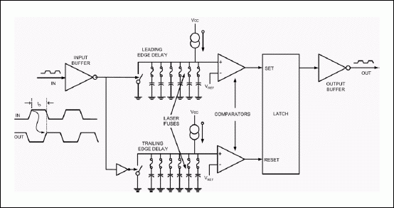
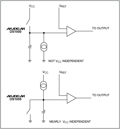
Old Generation DS1000 Delay Line.
The first Dallas delay lines consisted of a RC-based ramp generator and a comparator circuit that transitioned the delay line output when a certain voltage level of the ramp generator was reached. Calibration was performed at the factory at wafer level by using a laser to blow a series of fuses until the desired delay was achieved. There was no provision for temperature compensation.
Today, the current generation of lines is more sophisticated. Maxim/Dallas all-silicon delay lines contain a novel circuit consisting of a voltage-controlled delay line (VCDL) used in conjunction with a compensation circuit to reduce delay variations caused by changes in process, temperature, and voltage.
Building a silicon delay line is not very difficult. Any logic gate has a propagation delay and can be used as a delay line. The difficult part is building a delay line that can be set precisely to a specific delay period that remains consistent over variations in process, temperature, and voltage. Stabilizing these delay times requires a compensation scheme independent of these parameters.
One way to do this is to use feedback, determine a delay error and use that error to generate a corrective input back into the delay line. This requires a method to measure the delay error and a way to control the delay time. A simple way to control the delay time in a logic gate is to vary the supply voltage. In general, the higher the voltage, the shorter the delay through the gate.
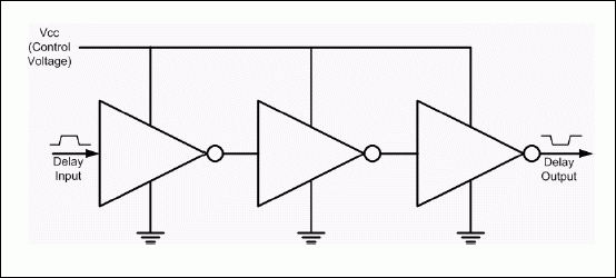
Figure 1. Voltage-controlled delay line (VCDL).
More work is required to measure the delay time and determine the delay error. The easiest method to the measure delay time is to convert it to something more easily measured, like frequency. If you take the output from delay line, invert it and feed it back into its input you have an oscillator with a frequency 1/2td, where td is the total delay through the delay lines. In this case, we have a voltage-controlled oscillator (VCO) based on a VCDL (Figure 2).
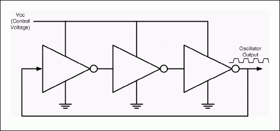
Figure 2. VCO based on a VCDL.
If we had a precise frequency reference (which we do not) a phase-locked loop could be implemented to lock the VCO frequency to the reference frequency, giving it the same precision. This is called a delay-lock loop (DLL). Other references are available in the silicon world, such as voltage references, that can be calibrated at the time of production to very precise levels.
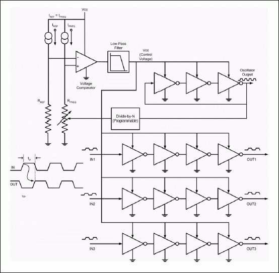
Given this, we have all the elements to build a compensated delay line. Figure 3 shows a block diagram for a DS1135 3-in-1 delay line.

Figure 3. Delay line (DS1135) based on delay-lock loop technology.
In the circuit (Figure 3), the oscillator output is fed back into a voltage-controlled resistance biased by a fixed current source. The controlled resistance is actually a switched capacitor circuit that has a DC resistance inversely proportional to the frequency of the feedback. As the frequency increases, the voltage drops. This voltage is compared to a fixed-voltage reference consisting of a matched current source and a fixed resistance (Rref). Rfreq is calibrated to match the characteristics of Rref over temperature and voltage. The output of the comparator is filtered and provides the VCO'fs drive voltage. As frequency increases, Vfreq decreases with respect to Vref, decreasing the drive voltage into the VCO, reducing the frequency. As the frequency decreases, the opposite happens, increasing the frequency. The stability of the frequency is equal to the stability of Rref. Rref is a precision reference that is stable over voltage and temperature and voltage. The control loop forces Rfreq to equal Rref. This control loop also negates changes in the delay portion of the circuit caused by variations in process, temperature, and voltage.
But this circuit alone cannot be used as a delay line. It does make a stable oscillator and is the circuit used in Dallas Semiconductors EconOscillators™. Fortunately, delay cells on the same piece of silicon, have nearly identical characteristics to the delay cell used in the VCO (Figure 3). The control voltage fed into the VCDL (configured as a VCO) has an identical effect on these other independent delay cells. So even though they are operating open loop, the control voltage applied to them has the same effect that is has on the delay cell configured in the VCO providing compensation for changes caused by process, temperature, and voltage.
These individual delay cells can be daisy chained together and make a tapped delay line like the DS1100, or they can be used independently as they are in the DS1135. The DS1077 EconOscillators uses the oscillator section only in conjunction with a programmable divider chain to give a customer-configurable all silicon oscillator. Combine this circuit with a DAC controlling the VCO's control voltage and a full-scale frequency synthesizer like the DS1085 is produced.
The circuitry described above is patented by Dallas Semiconductor (U.S. patent 5,982,241, as well as other patents).
How Do Dallas Semiconductor Delay Lines Work?
In the early eighties, Dallas Semiconductor was the first company to develop the all-silicon delay line. This provided a smaller, more cost-effective alternative to the modular delay lines used at the time.
Old Generation DS1000 Delay Line.
The first Dallas delay lines consisted of a RC-based ramp generator and a comparator circuit that transitioned the delay line output when a certain voltage level of the ramp generator was reached. Calibration was performed at the factory at wafer level by using a laser to blow a series of fuses until the desired delay was achieved. There was no provision for temperature compensation.
Today, the current generation of lines is more sophisticated. Maxim/Dallas all-silicon delay lines contain a novel circuit consisting of a voltage-controlled delay line (VCDL) used in conjunction with a compensation circuit to reduce delay variations caused by changes in process, temperature, and voltage.
Building a silicon delay line is not very difficult. Any logic gate has a propagation delay and can be used as a delay line. The difficult part is building a delay line that can be set precisely to a specific delay period that remains consistent over variations in process, temperature, and voltage. Stabilizing these delay times requires a compensation scheme independent of these parameters.
One way to do this is to use feedback, determine a delay error and use that error to generate a corrective input back into the delay line. This requires a method to measure the delay error and a way to control the delay time. A simple way to control the delay time in a logic gate is to vary the supply voltage. In general, the higher the voltage, the shorter the delay through the gate.

Figure 1. Voltage-controlled delay line (VCDL).
More work is required to measure the delay time and determine the delay error. The easiest method to the measure delay time is to convert it to something more easily measured, like frequency. If you take the output from delay line, invert it and feed it back into its input you have an oscillator with a frequency 1/2td, where td is the total delay through the delay lines. In this case, we have a voltage-controlled oscillator (VCO) based on a VCDL (Figure 2).

Figure 2. VCO based on a VCDL.
If we had a precise frequency reference (which we do not) a phase-locked loop could be implemented to lock the VCO frequency to the reference frequency, giving it the same precision. This is called a delay-lock loop (DLL). Other references are available in the silicon world, such as voltage references, that can be calibrated at the time of production to very precise levels.
Given this, we have all the elements to build a compensated delay line. Figure 3 shows a block diagram for a DS1135 3-in-1 delay line.

Figure 3. Delay line (DS1135) based on delay-lock loop technology.
In the circuit (Figure 3), the oscillator output is fed back into a voltage-controlled resistance biased by a fixed current source. The controlled resistance is actually a switched capacitor circuit that has a DC resistance inversely proportional to the frequency of the feedback. As the frequency increases, the voltage drops. This voltage is compared to a fixed-voltage reference consisting of a matched current source and a fixed resistance (Rref). Rfreq is calibrated to match the characteristics of Rref over temperature and voltage. The output of the comparator is filtered and provides the VCO'fs drive voltage. As frequency increases, Vfreq decreases with respect to Vref, decreasing the drive voltage into the VCO, reducing the frequency. As the frequency decreases, the opposite happens, increasing the frequency. The stability of the frequency is equal to the stability of Rref. Rref is a precision reference that is stable over voltage and temperature and voltage. The control loop forces Rfreq to equal Rref. This control loop also negates changes in the delay portion of the circuit caused by variations in process, temperature, and voltage.
But this circuit alone cannot be used as a delay line. It does make a stable oscillator and is the circuit used in Dallas Semiconductors EconOscillators™. Fortunately, delay cells on the same piece of silicon, have nearly identical characteristics to the delay cell used in the VCO (Figure 3). The control voltage fed into the VCDL (configured as a VCO) has an identical effect on these other independent delay cells. So even though they are operating open loop, the control voltage applied to them has the same effect that is has on the delay cell configured in the VCO providing compensation for changes caused by process, temperature, and voltage.
These individual delay cells can be daisy chained together and make a tapped delay line like the DS1100, or they can be used independently as they are in the DS1135. The DS1077 EconOscillators uses the oscillator section only in conjunction with a programmable divider chain to give a customer-configurable all silicon oscillator. Combine this circuit with a DAC controlling the VCO's control voltage and a full-scale frequency synthesizer like the DS1085 is produced.
The circuitry described above is patented by Dallas Semiconductor (U.S. patent 5,982,241, as well as other patents).
EconOscillator is a trademark of Maxim Integrated Products, Inc.
 电子发烧友App











评论