Abstract: This application brief discusses the architectural and structural differences between solid-state and hybrid delay lines. In many cases, solid-state delay lines provide a functional, if not pin-for-pin, replacement for hybrid delay lines at a lower cost, in smaller lighter packages, and with higher reliability. The article outlines the operation of older, modular delay lines and explains how this same functionality is performed using these all-silicon replacements.
Important functional and parametric differences are discussed to give the electronics designer an overview and understanding of silicon delay line technology to simplify the integration into new and existing designs requiring or already using delay line technology.
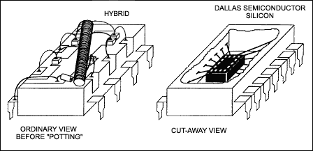
Figure 1. Internal views.
By comparison, the silicon delay line consists of a laser-optimized die bonded to a conventional lead frame molded into an auto-insertable industry standard DIP or surface-mount SOIC package. The die is a low-power CMOS design fabricated on 6-inch wafers by Dallas Semiconductor's Class 1 facility. Using lasers for late definition of finished wafers provides both economy and maximum flexibility; both rising and falling edges can be programmed to standard or custom delays over a wide range of values. A post-laser final passivation step protects against contamination by covering the laser fuse windows before packaging.
The basic building block of a silicon delay line consists of a ramp generator with associated logic (Figure 2). The input signal triggers a ramp generator that supplies a laser-adjusted voltage-to-time relationship (Figures 3 and 4). A comparator is used to detect the ramp reaching the reference voltage (VREF); this sets or resets the output latch. The DS1013 family has three independent blocks in parallel while the DS1000, DS1005, and DS1010 families have the blocks connected in series with a single external input (Figure 5). All silicon delay lines, unlike most TTL-based hybrids, have true CMOS output levels.

Figure 2. Basic building block.
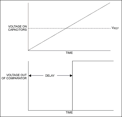
Figure 3. Voltage to time conversion.
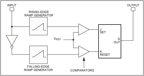
Figure 4. Expanded basic block.
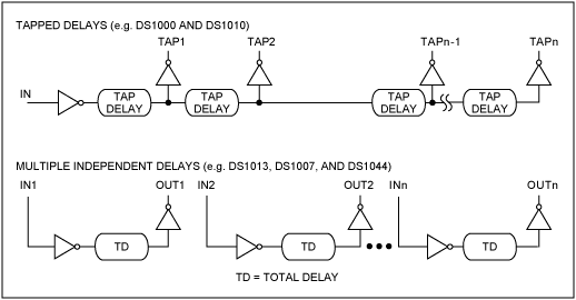
Figure 5. Delay line families.
The linear ramp generator is implemented with constant current sources charging capacitors (Figure 6). By using a combination of several large current sources and capacitors and binary weighted smaller current sources and capacitors, maximum flexibility with subnanosecond adjustment is obtained on a single silicon die (Figure 7). Under the direction of a computer-controlled tester with 20-picosecond resolution, the proper slope of the ramp (Figure 8) is obtained by directing a laser to remove the unnecessary current sources and capacitors. This is accomplished by opening polysilicon fuses (Figure 9).
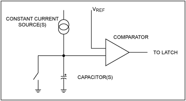
Figure 6. Basic ramp generator.
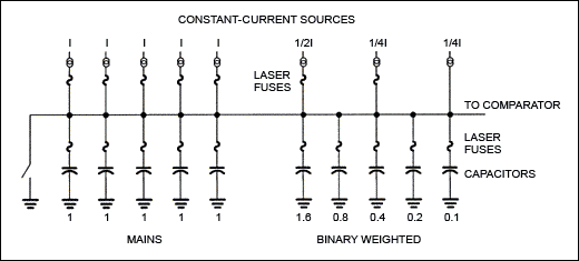
Figure 7. Laser programmable elements.
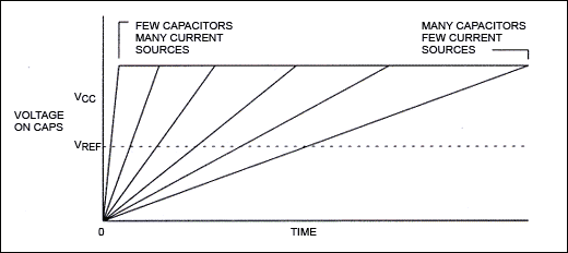
Figure 8. Range of adjustment.
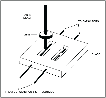
Figure 9. Laser blowing polysilicon fuse.
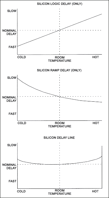
Figure 10. Delay vs. temperature.
Timing on hybrid lines is determined by coil winding and/or capacitor selection or trimming. Achieving both rising and falling edge accuracy at the same time is difficult and comes at a premium price. Furthermore, timing is subject to the variations of the 74LS04 devices procured from other manufacturers. On silicon delay lines, temperature compensation is implemented by balancing the positive temperature coefficient of the CMOS logic against the negative coefficient of the ramp generator. Figure 10 shows that the logic portion of the circuit, like hybrid delay lines in general, slows linearly with increasing temperature. Since the ramp speeds up nonlinearly, the two effects tend to cancel, minimizing the effects of temperature. Because the net result resembles a parabolic shape, temperature coefficients specified in parts per million (ppm) are inappropriate to describe the behavior of silicon delay lines. A more meaningful parameter is maximum shift from nominal anywhere over the rated temperature range. Figure 11 compares the two technologies over temperature. While some silicon delay line families (DS1000 and DS1010) provide minimal voltage independence (4% delay change for 5% supply variation), the newer designs (DS1005 and DS1013) provide a higher degree of supply isolation (= < 1% delay change for 5% supply variation). The newer designs achieve supply voltage independence by employing positive ramps referenced to ground rather than negative ramps referenced to VCC (Figure 12).
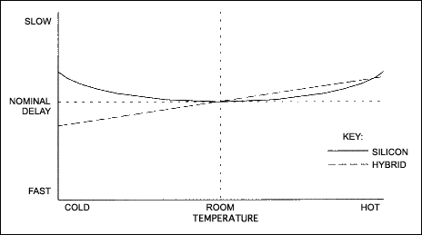
Figure 11. Hybrid vs. silicon over temperature.
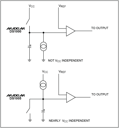
Figure 12. Comparison of delay designs.
While hybrids offer little flexibility in packaging, silicon lines are available in a variety of industry standard DIP and SOIC packages (See Packaging Options below). To maintain compatibility with existing designs based on hybrids having missing pins, a clipped lead version is offered. Finally, for surface mount applications, two solutions are available: 300mil DIPs with the leads trimmed and "gull winged," and industry standard SOIC packages.
Table 1 summarizes some of the disadvantages of the hybrid design and some of the advantages of the silicon solution.
Table 1.
Straight lead:
This is the conventional package and is used for through-hole mounting in PCBs.
Gullwing:
The leads are formed to sit flat on the surface of a PCB for surface mount applications.
Sheared NC
All "no connect" (NC) leads are sheared off the package. This package is commonly used for hybrid replacement applications.
Note:
The use of gullwing or sheared NC packages is not encouraged for new designs; however, these packages will continue to be made available for existing designs.
* Default package, no letter designator required.
Tape and reel packaging is also available; contact the factory for more information.
Important functional and parametric differences are discussed to give the electronics designer an overview and understanding of silicon delay line technology to simplify the integration into new and existing designs requiring or already using delay line technology.
Silicon Delay Lines vs. Hybrid L-C Networks
Figure 1 shows internal views of a typical 5-tap hybrid delay line and its silicon counterpart. A hybrid is manufactured using a commercially available hex inverter DIP (e.g., 74LS04) with a small PC board placed on top to supply a ground plane. Next, several leads are bent up and over the top of the PC board. Five chip capacitors and a terminating resistor are soldered to the ground plane and a 5-tap ferrite inductor is positioned above. Note that nearly two dozen solder joints are required to electrically connect the various components. Finally, the entire assembly is placed into an oversized plastic tub and filled with a potting material.
Figure 1. Internal views.
By comparison, the silicon delay line consists of a laser-optimized die bonded to a conventional lead frame molded into an auto-insertable industry standard DIP or surface-mount SOIC package. The die is a low-power CMOS design fabricated on 6-inch wafers by Dallas Semiconductor's Class 1 facility. Using lasers for late definition of finished wafers provides both economy and maximum flexibility; both rising and falling edges can be programmed to standard or custom delays over a wide range of values. A post-laser final passivation step protects against contamination by covering the laser fuse windows before packaging.
The basic building block of a silicon delay line consists of a ramp generator with associated logic (Figure 2). The input signal triggers a ramp generator that supplies a laser-adjusted voltage-to-time relationship (Figures 3 and 4). A comparator is used to detect the ramp reaching the reference voltage (VREF); this sets or resets the output latch. The DS1013 family has three independent blocks in parallel while the DS1000, DS1005, and DS1010 families have the blocks connected in series with a single external input (Figure 5). All silicon delay lines, unlike most TTL-based hybrids, have true CMOS output levels.

Figure 2. Basic building block.

Figure 3. Voltage to time conversion.

Figure 4. Expanded basic block.

Figure 5. Delay line families.
The linear ramp generator is implemented with constant current sources charging capacitors (Figure 6). By using a combination of several large current sources and capacitors and binary weighted smaller current sources and capacitors, maximum flexibility with subnanosecond adjustment is obtained on a single silicon die (Figure 7). Under the direction of a computer-controlled tester with 20-picosecond resolution, the proper slope of the ramp (Figure 8) is obtained by directing a laser to remove the unnecessary current sources and capacitors. This is accomplished by opening polysilicon fuses (Figure 9).

Figure 6. Basic ramp generator.

Figure 7. Laser programmable elements.

Figure 8. Range of adjustment.

Figure 9. Laser blowing polysilicon fuse.

Figure 10. Delay vs. temperature.
Timing on hybrid lines is determined by coil winding and/or capacitor selection or trimming. Achieving both rising and falling edge accuracy at the same time is difficult and comes at a premium price. Furthermore, timing is subject to the variations of the 74LS04 devices procured from other manufacturers. On silicon delay lines, temperature compensation is implemented by balancing the positive temperature coefficient of the CMOS logic against the negative coefficient of the ramp generator. Figure 10 shows that the logic portion of the circuit, like hybrid delay lines in general, slows linearly with increasing temperature. Since the ramp speeds up nonlinearly, the two effects tend to cancel, minimizing the effects of temperature. Because the net result resembles a parabolic shape, temperature coefficients specified in parts per million (ppm) are inappropriate to describe the behavior of silicon delay lines. A more meaningful parameter is maximum shift from nominal anywhere over the rated temperature range. Figure 11 compares the two technologies over temperature. While some silicon delay line families (DS1000 and DS1010) provide minimal voltage independence (4% delay change for 5% supply variation), the newer designs (DS1005 and DS1013) provide a higher degree of supply isolation (= < 1% delay change for 5% supply variation). The newer designs achieve supply voltage independence by employing positive ramps referenced to ground rather than negative ramps referenced to VCC (Figure 12).

Figure 11. Hybrid vs. silicon over temperature.

Figure 12. Comparison of delay designs.
While hybrids offer little flexibility in packaging, silicon lines are available in a variety of industry standard DIP and SOIC packages (See Packaging Options below). To maintain compatibility with existing designs based on hybrids having missing pins, a clipped lead version is offered. Finally, for surface mount applications, two solutions are available: 300mil DIPs with the leads trimmed and "gull winged," and industry standard SOIC packages.
Table 1 summarizes some of the disadvantages of the hybrid design and some of the advantages of the silicon solution.
Table 1.
| Disadvantage of Hybrids | Advantages of Silicon |
|
|
|
Package Options
Dual-In-Line (DIP)
DIP packages are available in pin counts of 8, 14 and 16 pins. Three lead-forming options are available:Straight lead:
This is the conventional package and is used for through-hole mounting in PCBs.
Gullwing:
The leads are formed to sit flat on the surface of a PCB for surface mount applications.
Sheared NC
All "no connect" (NC) leads are sheared off the package. This package is commonly used for hybrid replacement applications.
Note:
The use of gullwing or sheared NC packages is not encouraged for new designs; however, these packages will continue to be made available for existing designs.
Small Outline (SOIC)
Small outline surface mount packages are available in pin counts of 8, 14 and 16 pins. Two package widths are also available: 150mil and 300mil.| Package Availability / Letter Designations | |||||
| # Pins | DIP | SOIC | |||
| STD | Gullwing | Sheared | 150mil | 300mil | |
| 8 | M | H | Z | ||
| 14 | none* | G | K | R | |
| 16 | S | ||||
Tape and reel packaging is also available; contact the factory for more information.
 电子发烧友App






评论