Abstract: This application note looks at the new serial port features found in the Dallas Semiconductor DS89C430 and DS89C450 ultra high-speed microcontrollers. The addition of a clock multiplier allows the user to benefit by selecting a crystal at one-forth the original frequency to produce the same baud rates with reduced EMI.
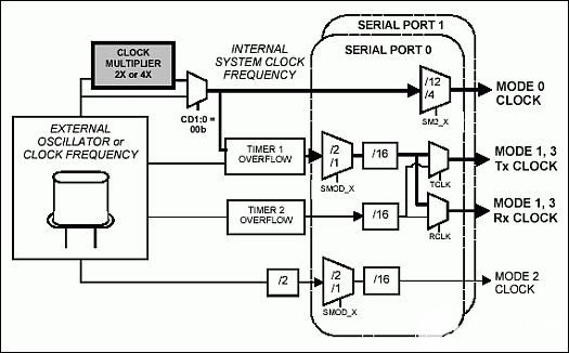
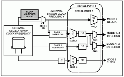
Once the clock multiplier output has been selected (CD1:0 = 00b) as the internal system clock, certain serial port baud clocks derived from the system clock (no longer equal to the external oscillator frequency) will change. Figure 1 highlights the serial port clocks potentially affected when using the 2X or 4X multiplied system clock. The Serial Mode 0 baud rate will always differ, Serial Mode 2 baud rate will never differ, and the Serial Mode 1, 3 baud rates can differ, depending upon the timer used and/or timer input clock selection. Table 1, as per Figure 1, denotes which serial port modes are affected by use of the clock multiplier. Appendix A contains detailed equations for performing baud rate calculations when using the 2X or 4X clock multiplier mode.

Figure 1. Serial port clocks affected by selection of the clock multiplier output (CD1:0 = 00b).
Table 1. Serial port baud clocks dependent on the system clock
¹ Only when the divide by 4 or divide by 1 Timer 1 input clock is enabled (T1M = 1 or T1MH = 1). For compatibility with the original 8051, the default Timer 1 input clock (T1MH, T1M = 00b) is fixed to the oscillator clock divided by 12.
² Available for baud rate generation on Serial Port 0 only.
The T0MH, T1MH, and T2MH bits, contained in the CKMOD (96h) SFR, respectively enable the system clock divide by 1 input to Timer 0, Timer 1, and Timer 2. Enabling the high-speed system-clock input to the timer (TxMH = 1) will automatically override the system clock divided by 4 input (TxM = 1) setting. The new system clock divide by 1 timer input, like the system clock divide by 4 input, factors into baud rate generation when using Timer 1. Figure 2 highlights the serial port clocks potentially affected by selection of the high-speed clock input to Timer 1.

Figure 2. Serial port clocks affected by selection of high-speed timer 1 input (T1MH = 1).
For example, suppose a user currently has a Dallas high-speed microcontroller application running at a 20MHz system clock frequency. The application uses one of the serial ports for RS232 communication with a PC, and requires that the baud rate mismatch between the two be < 3%. If using Timer 1 (in the 8-bit auto-reload mode) for baud rate generation, Table 2 below gives a sampling of the "good" baud rates for the Dallas high-speed microcontroller versus those for the new Ultra High Speed Microcontrolle. The unacceptable baud rates (those with mismatch > 3%) have been shaded in gray. Table 3 makes the same "good" baud rate comparison for a system clock frequency of 25MHz. As one can plainly see, enabling the high-speed Timer 1 input clock gives much finer baud rate resolution. Appendix A contains detailed equations for performing baud rate calculations when utilizing the system clock input to Timer 1 (T1MH = 1).
Table 2. High-speed microcontroller vs. ultra high-speed microcontroller timer 1 baud rate generation capability (SYSCLK = 20MHz)
Table 3. High-speed microcontroller vs. ultra high-speed microcontroller timer 1 baud rate generation capability (SYSCLK = 25MHz)

Figure 3. Example serial port interface to an spi-compatible peripheral.
Serial Port 0 is first placed into Mode 0 and configured to produce a system clock divide by 4 baud clock. Depending upon the timing restrictions of the attached SPI peripheral, a reduced system clock or system clock divide by 12 baud clock may need to be selected. Externally, the TXD pin (P3.1) provides the serial clock and connects to the SCK input of the EEPROM. The RXD pin (P3.0) handles all SPI data transactions via its connection to both the SI input and SO output of the EEPROM. The ability to use a shared SI/SO configuration will depend upon the I/O timing of the attached SPI peripheral. A third microcontroller port pin, not linked to the on-chip serial port hardware, serves as the SPI peripheral chip select input. In this example, port pin P3.2 will be connected to the EEPROM active-low CS input and will be manually asserted and de-asserted by the software. Since the serial port communicates LSB first and the SPI peripheral expects to communicate MSB first, a lookup table is used for byte translation in most cases.
Two routines, XRAM_store and XRAM_recall, have been created and do exactly as their names would simply. The XRAM_store routine writes the current contents of the internal 1kB SRAM to a specified 1kB range of EEPROM, while XRAM_recall reads the specified 1kB range of EEPROM into the DS89C430 on-chip SRAM. This code is intended only as an example and could easily be adapted to access different address ranges of the microcontroller or EEPROM memory, in smaller or larger blocks.

Figure 4. Example RS-485 networking using hardware serial port interfaces.
The figure above diagrams an RS-485 network interface between (3) DS89C430 microcontrollers. The asynchronous serial modes use the TXD pin for transmission and the RXD pin for reception. These pins connect directly to the DI (data input) and RO (receive output) pins of the RS-485 transceiver. A third microcontroller port pin, P1.4, is connected to both the DE (data enable) and active-low RE (receive enable) and will serve as the directional control for the half-duplex transceiver. The network uses a master/slave architecture (1 master, 2 slaves), where each slave device has its own unique address and must first be addressed by the master before transmitting on the bus. All devices are operated at a 22.1184MHz system clock frequency and use Timer 1 to produce a 1.38M baud rate. The settings needed to generate this baud rate can be found in Table 4 following the figure.
Table 4. Asynchronous mode 1, 3 baud rate vs. system clock (RLCK = 0, TCLK = 0, T1MH = 1, SMOD_x = 1)
¹ Baud rate used in Application Example #2.
² The clock multiplier is used for illustration and is not required to generate these system clock frequencies.
Overview
In contrast to the original 8051 architecture that required a minimum of 12 clocks per instruction cycle, the Ultra High-Speed Microcontroller features an advanced 8051 core architecture capable of executing instructions in as little as one clock cycle. To complement the high performance core, new hardware features were integrated into the standard 8051 on-chip peripherals. Two of the new features, the clock multiplier and selectable high-speed clock to the timers, can directly affect baud rate generation for the serial ports. The purpose of this document is to explain the interaction between these two new features and serial-port baud-rate generation.Serial Port Modes
The DS89C430 serial ports offer four basic modes of operation. Mode 0 allows half-duplex synchronous communication of 8-bit data using a baud clock derived from the system clock. Mode 1 allows fullduplex asynchronous communication of 8-bit data with a baud clock derived from Timer 1 or Timer 2. Mode 3 differs from Mode 1 by supporting 9-bit data transmission and reception. Mode 2 similarly provides 9-bit data communication, but instead derives its baud clock directly from the oscillator frequency. To support Mode 1, 2, and 3 asynchronous communication, a start bit always precedes the data and a stop bit always follows. Full details of each serial port mode can be found in the Ultra High Speed Microcontroller User's Guide.Clock Multiplier
The Ultra High Speed Microcontroller incorporates an on-chip clock multiplier to give increased performance at a reduced external crystal clock frequency. The multiplier can be configured to generate either a doubled (2X) or quadrupled (4X) internal system clock, controlled by the 2X/4X special function register bit (PMR.3). Please note that the resultant 2X or 4X multiplied system clock still cannot exceed the maximum operating frequency specified in the data sheet. Full details pertaining to the multiplier can be found in the Ultra High Speed Microcontroller User's Guide.Once the clock multiplier output has been selected (CD1:0 = 00b) as the internal system clock, certain serial port baud clocks derived from the system clock (no longer equal to the external oscillator frequency) will change. Figure 1 highlights the serial port clocks potentially affected when using the 2X or 4X multiplied system clock. The Serial Mode 0 baud rate will always differ, Serial Mode 2 baud rate will never differ, and the Serial Mode 1, 3 baud rates can differ, depending upon the timer used and/or timer input clock selection. Table 1, as per Figure 1, denotes which serial port modes are affected by use of the clock multiplier. Appendix A contains detailed equations for performing baud rate calculations when using the 2X or 4X clock multiplier mode.

Figure 1. Serial port clocks affected by selection of the clock multiplier output (CD1:0 = 00b).
Table 1. Serial port baud clocks dependent on the system clock
| SERIAL PORT MODE | BAUD CLOCK SOURCE | BAUD CLOCK DEPENDENT ON THE INTERNAL SYSTEM CLOCK (CLOCK MULTIPLIER SELECTION) |
| Mode 0 (synchronous - 8 bits) |
System Clock/4 System Clock/12 |
YES |
| Mode 1 (asynchronous - 10 bits) |
Timer 1 Timer 2 |
YES¹ NO² |
| Mode 2 (asynchronous - 11 bits) |
Oscillator Clock/32 Oscillator Clock/64 |
NO |
| Mode 3 (asynchronous - 11 bits) |
Timer 1 Timer 2 |
YES¹ NO² |
² Available for baud rate generation on Serial Port 0 only.
Benefits: Faster Baud Rates, Reduced EMI
When using the clock multiplier, the application benefits can be great. An external crystal clock of onefourth the original frequency can be used to produce the same Serial Mode 0 and (Timer 1 generated) Mode 1, 3 baud rates as before, but with much reduced EMI. Alternatively, the same external crystal, when multiplied internally by 2X or 4X, can now generate baud clocks up to four times faster!High-Speed Input Clock to Timers
In order for the on-chip timers to be most useful to the application, each should be able to track time at a rate equivalent to the minimum instruction cycle. For the original 8051 architecture, which executed instructions in 12 oscillator clocks, the timers were clocked at an oscillator frequency divided by 12 rate. When Dallas Semiconductor introduced its high-speed microcontroller with a reduced machine cycle of four oscillator clocks, a selectable oscillator frequency divided by 4 input-clock control was provided for each timer. When the clock multiplier function was added to the high-speed microcontroller family, the selectable divide by 4 timer-input clock was modified to become a function of the system clock, not the oscillator clock. Now, the Ultra High-Speed Microcontroller boasts single clock-cycle instruction execution. Once again, each of the on-chip timers has been upgraded with the integration of a selectable system clock divide by 1 input.The T0MH, T1MH, and T2MH bits, contained in the CKMOD (96h) SFR, respectively enable the system clock divide by 1 input to Timer 0, Timer 1, and Timer 2. Enabling the high-speed system-clock input to the timer (TxMH = 1) will automatically override the system clock divided by 4 input (TxM = 1) setting. The new system clock divide by 1 timer input, like the system clock divide by 4 input, factors into baud rate generation when using Timer 1. Figure 2 highlights the serial port clocks potentially affected by selection of the high-speed clock input to Timer 1.

Figure 2. Serial port clocks affected by selection of high-speed timer 1 input (T1MH = 1).
Benefits: Faster Baud Rates, Increased Baud Rate Resolution
Relative to serial port operation, the divide by 1 input-clock feature translates into two user benefits. First, provided with the same system clock frequency, baud rates four times faster can now be generated for Serial Modes 1 and 3 when using Timer 1. Secondly, clocking Timer 1 faster allows higher baud rate resolution, potentially reducing error associated with baud rates already used by the application, or bringing new baud rates within an acceptable error range for application use.For example, suppose a user currently has a Dallas high-speed microcontroller application running at a 20MHz system clock frequency. The application uses one of the serial ports for RS232 communication with a PC, and requires that the baud rate mismatch between the two be < 3%. If using Timer 1 (in the 8-bit auto-reload mode) for baud rate generation, Table 2 below gives a sampling of the "good" baud rates for the Dallas high-speed microcontroller versus those for the new Ultra High Speed Microcontrolle. The unacceptable baud rates (those with mismatch > 3%) have been shaded in gray. Table 3 makes the same "good" baud rate comparison for a system clock frequency of 25MHz. As one can plainly see, enabling the high-speed Timer 1 input clock gives much finer baud rate resolution. Appendix A contains detailed equations for performing baud rate calculations when utilizing the system clock input to Timer 1 (T1MH = 1).
Table 2. High-speed microcontroller vs. ultra high-speed microcontroller timer 1 baud rate generation capability (SYSCLK = 20MHz)
| PC UART (8250/16450) | HIGH-SPEED MICROCONTROLLER (Timer 1 with T1M = 1 used for baud rate generation, SMOD_x = 1) | ULTRA HIGH-SPEED MICROCONTROLLER (Timer 1 with T1MH = 1 used for baud rate generation, SMOD_x = 1) | |||
| Reload | Baud Rate | Baud Rate (TH1) | % Error | Baud Rate (TH1) | Error |
| 1 | 115200 | 104166 (FD) | -9.6 | 113636 (F5) | -1.4 |
| 2 | 57600 | 62500 (FB) | 8.5 | 56818 (EA) | -1.4 |
| 3 | 38400 | 39062 (F8) | 1.7 | 37879 (DF) | -1.4 |
| 4 | 28800 | 28409 (F5) | -1.4 | 29070 (D5) | 0.9 |
| 5 | 23040 | 22321 (F2) | -3.1 | 23148 (CA) | 0.5 |
| 6 | 19200 | 19531 (F0) | 1.7 | 19231 (BF) | 0.2 |
| 7 | 16457 | 16447 (ED) | -0.1 | 16447 (B4) | -0.1 |
| 8 | 14400 | 14204 (EA) | -1.4 | 14368 (A9) | -0.2 |
| 9 | 12800 | 13020 (E8) | 1.7 | 12755 (9E) | -0.4 |
| 10 | 11520 | 11574 (E5) | 0.5 | 11574 (94) | 0.5 |
| 11 | 10472 | 10417 (E2) | -0.5 | 10417 (88) | -0.5 |
| 12 | 9600 | 9469 (DF) | -1.4 | 9615 (7E) | 0.2 |
Table 3. High-speed microcontroller vs. ultra high-speed microcontroller timer 1 baud rate generation capability (SYSCLK = 25MHz)
| PC UART (8250/16450) |
HIGH-SPEED MICROCONTROLLER (Timer 1 with T1M = 1 used for baud rate generation, SMOD_x = 1) |
ULTRA HIGH-SPEED MICROCONTROLLER (Timer 1 with T1MH = 1 used for baud rate generation, SMOD_x = 1) | |||
| Reload | Baud Rate | Baud Rate (TH1) | % Error | Baud Rate (TH1) | Error |
| 1 | 115200 | 130208 (FD) | 13.0 | 111607 (F2) | -3.1 |
| 2 | 57600 | 55803 (F9) | -3.1 | 57870 (E5) | 0.4 |
| 3 | 38400 | 39062 (F6) | 1.7 | 38110 (D7) | -0.8 |
| 4 | 28800 | 27901 (F2) | -3.1 | 28935 (CA) | 0.5 |
| 5 | 23040 | 22978 (EF) | -0.3 | 22978 (BC) | -0.3 |
| 6 | 19200 | 19531 (EC) | 1.7 | 19290 (AF) | 0.5 |
| 7 | 16457 | 16276 (E8) | -1.1 | 16447 (A1) | -0.1 |
| 8 | 14400 | 14467 (E5) | 0.5 | 14335 (93) | -0.5 |
| 9 | 12800 | 12600 (E1) | -1.6 | 12807 (86) | 0.1 |
| 10 | 11520 | 11489 (DE) | -0.3 | 11489 (78) | -0.3 |
| 11 | 10472 | 10557 (DB) | 0.8 | 10487 (6B) | 0.1 |
| 12 | 9600 | 9527 (D7) | -0.8 | 9586 (5D) | -0.1 |
Application Example #1
SPI Mode (1,1) Interface Using Synchronous Serial Mode 0
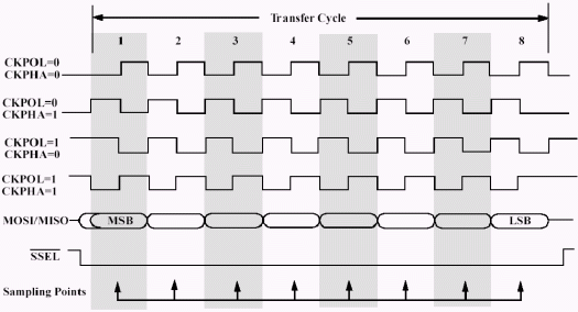
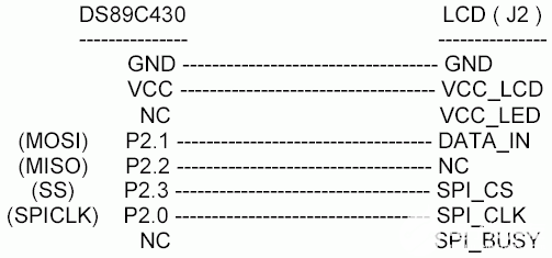
While one can interface to an SPI™ device by "bit-banging" port pins, using synchronous Serial Mode 0 reduces software overhead and allows faster communication speed. The synchronous serial mode of operation provides a shift clock on the TXD pin and writes/reads serial data on the RXD pin at each rising edge of the shift clock (TXD). Since TXD idles in the high state, the synchronous serial mode aligns closely with the CPOL = 1, CPHA = 1 SPI Mode. Since the synchronous serial mode does not require a 3-sample majority-voting scheme for each bit (like the asynchronous serial modes), it is capable of achieving baud rates faster than any other serial mode. The figure below illustrates an interface between the DS89C430 microcontroller and an SPI mode (1,1) compatible EEPROM device.
Figure 3. Example serial port interface to an spi-compatible peripheral.
Serial Port 0 is first placed into Mode 0 and configured to produce a system clock divide by 4 baud clock. Depending upon the timing restrictions of the attached SPI peripheral, a reduced system clock or system clock divide by 12 baud clock may need to be selected. Externally, the TXD pin (P3.1) provides the serial clock and connects to the SCK input of the EEPROM. The RXD pin (P3.0) handles all SPI data transactions via its connection to both the SI input and SO output of the EEPROM. The ability to use a shared SI/SO configuration will depend upon the I/O timing of the attached SPI peripheral. A third microcontroller port pin, not linked to the on-chip serial port hardware, serves as the SPI peripheral chip select input. In this example, port pin P3.2 will be connected to the EEPROM active-low CS input and will be manually asserted and de-asserted by the software. Since the serial port communicates LSB first and the SPI peripheral expects to communicate MSB first, a lookup table is used for byte translation in most cases.
Two routines, XRAM_store and XRAM_recall, have been created and do exactly as their names would simply. The XRAM_store routine writes the current contents of the internal 1kB SRAM to a specified 1kB range of EEPROM, while XRAM_recall reads the specified 1kB range of EEPROM into the DS89C430 on-chip SRAM. This code is intended only as an example and could easily be adapted to access different address ranges of the microcontroller or EEPROM memory, in smaller or larger blocks.
Code Listing: SPI Interface Using Synchronous Serial Port
;-------------------------------------------------------------- ; DS89C430 SPI I/F example code ; ; 420 pin SPI I/F pin ; --------- ----------- ; P3.2 Active-Low CS ; P3.1/TXD SCK ; P3.0/RXD SI,SO ;-------------------------------------------------------------- $include(420.def) ;SFR equates ee_cs bit p3.2 ;EEPROM Active-Low CS ;-------------------------------------------------------------- ; SPI EEPROM opcodes – (CAT25C64 used) ; ; (bits in each byte are reversed since serial communication ; is lsb-first whereas SPI communication is msb-first). ;-------------------------------------------------------------- ee_wren equ 01100000b ;=06h ee_rdsr equ 10100000b ;=05h ee_read equ 11000000b ;=03h ee_write equ 01000000b ;=02h ;-------------------------------------------------------------- ; constants ;-------------------------------------------------------------- eepg equ 64d ;64byte page writes (CAT25C64) xdb equ 1024d ;1KB xdata block ;-------------------------------------------------------------- ; Main Program ;-------------------------------------------------------------- org 0000h ;-------------------------------------------------------------- ; Serial Port 0: Mode 0, baud clock=sysclk/4 ; (Note: Tested @ sysclk = 25 MHz; SPI baud clock = 6.25 MHz. ; A reduced system clock frequency or sysclk/12 baud clock ; may be required depending on SPI device timing) ;-------------------------------------------------------------- mov scon, #20h ; mode 0, sysclk/4 clk ; mov scon, #00h ; mode 0, sysclk/12 clk ;-------------------------------------------------------------- ; XRAM store/recall example ;-------------------------------------------------------------- orl pmr, #01h ; Enable 1KB XRAM ;==> COPY CODE (0-03FFh) INTO XRAM DATA (0-03FFh) mov dps, #30h ; dptr auto-inc/togmov dptr, #0000h ; code dptr mov dptr, #0000h ; xram dptr copy: clr a movc a, @a+dptr ; read from code movx @dptr, a ; write to data mov a, dph cjne a, #04h, copy ; dptr=0400h yet? mov dps, #00h ; dptr auto-inc/tog ;==> STORE XRAM TO EEPROM BLOCK 0 (0000h - 03FFh) clr a ; a=00h (=EEPROM block 0) call XRAM_store ; store to EEPROM ;==> FILL XRAM WITH FFh DATA call fx ; fill XRAM with FFh data ;==> RECALL EEPROM BLOCK 0 (0000h - 03FFh) TO XRAM clr a ; a=00h (=EEPROM block 0) call XRAM_recall ; recall from EEPROM sjmp $ ;-------------------------------------------------------------- ; XRAM_store (a) ; acc: selects 1KB EEPROM block to store XRAM ; 00 -> 0000h-03FFh ; 01 -> 0400h-07FFh ; .. ; 07 -> 1C00h-1FFFh ; r5: local counter = pages left to write ;-------------------------------------------------------------- XRAM_store: mov dps, #01h ; dptr1= source (XRAM) mov dptr, #0000h ; dptr1= 0000h mov r5, #(xdb/eepg) ; 1024/64 = 16 rl a ; rotate block index left rl a ; twice to get msb addr mov dph, a ; dptr = dest (EEPROM) mov dpl, #00h write: call wren ; __________WREN___________ wel_wait: call rdsr ; __________RDSR___________ jnb acc.1, wel_wait ; poll for WEL bit = 1 clr ee_cs ; Active-Low CS = 0 mov sbuf, #ee_write ; __________WRITE__________ jnb ti, $ ; command sent clr ti mov a, dph ; get dest msb addr call bitrev ; use LUT to transpose byte mov sbuf, a ; __________ __________ jnb ti, $ ; sent clr ti mov a, dpl ; get dest lsb addr call bitrev ; use LUT to transpose byte mov sbuf, a ; __________ __________ jnb ti, $ ; sent clr ti orl dps, #30h ; dptr auto-inc/tog write_64: movx a, @dptr ; dptr1 XRAM read call bitrev ; use LUT to transpose byte mov sbuf, a ; ___________________ inc dptr ; inc dest dptr mov a, dpl ; check dest dptr for page anl a, #(eepg-1) ; write multiple (64d) jnb ti, $ ; sent clr ti jnz write_64 ; 64bytes written? setb ee_cs ; Active-Low CS=1 rdypoll: call rdsr ; __________RDSR___________ jb acc.0, rdypoll ; poll for RDY bit = 0 djnz r5, write ; all pages written? anl dps, #0cfh ; dptr auto-inc/tog ret ;-------------------------------------------------------------- ; XRAM_recall (a) ; acc: selects 1KB EEPROM block to copy into XRAM ; 00 -> 0000h-03FFh ; 01 -> 0400h-07FFh ; .. ; 07 -> 1C00h-1FFFh ; r5: local counter of 256byte pages left to read ;-------------------------------------------------------------- XRAM_recall: mov dps, #01h ; dptr1 = dest (XRAM) mov dptr, #0000h ; dptr1 = 0000h mov r5, #(xdb/256) ; 1024/256 = 4 rl a ; rotate block index left rl a ; twice to get msb addr clr ee_cs ; Active-Low CS = 0 mov sbuf, #ee_read ; __________READ___________ jnb ti, $ ; command sent clr ti call bitrev ; use LUT to transpose byte mov sbuf, a ; __________ __________ jnb ti, $ ; msb sent clr ti mov sbuf, #00h ; __________ __________ jnb ti, $ ; lsb sent clr ti setb ri ; don't receive yet setb ren ; enable receive orl dps, #10h ; dptr auto-inc read: clr ri ; ___________________ jnb ri, $ ; got data mov a, sbuf call bitrev ; use LUT to transpose byte movx @dptr, a ; dptr1 XRAM write mov a, dpl1 ; check dest dptr for 256 jnz read ; byte boundary djnz r5, read ; all pages read? clr ren ; disable receive clr ri setb ee_cs ; Active-Low CS = 1 anl dps, #0efh ; dptr auto-inc ret ;-------------------------------------------------------------- ; EEPROM commands: WREN, RDSR ;-------------------------------------------------------------- wren: clr ee_cs ; Active-Low CS = 0 mov sbuf, #ee_wren ; __________WREN___________ jnb ti, $ ; command sent clr ti setb ee_cs ; Active-Low CS = 1 ret rdsr: clr ee_cs ; Active-Low CS = 0 mov sbuf, #ee_rdsr ; __________RDSR___________ jnb ti, $ ; command sent clr ti setb ren ; enable receive jnb ri, $ ; got data clr ren ; disable receive clr ri setb ee_cs ; Active-Low CS = 1 mov a, sbuf call bitrev ; use LUT to transpose byte ret ;-------------------------------------------------------------- ; fill XRAM with FFh data ;-------------------------------------------------------------- fx: mov dps, #10h ; dptr auto-inc mov dptr, #0000h fx1: mov a, #0ffh movx @dptr, a mov a, dph cjne a, #04h, fx1 mov dps, #00h ; dptr auto-inc ret ;-------------------------------------------------------------- ; bit reversal LUT ;-------------------------------------------------------------- bitrev: jnz do_lookup ; no lookup if a=00h ret ; since 00h transposed = 00h do_lookup: movc a, @a+pc ret db 080h,040h,0C0h,020h,0A0h,060h,0E0h db 010h,090h,050h,0D0h,030h,0B0h,070h,0F0h db 008h,088h,048h,0C8h,028h,0A8h,068h,0E8h db 018h,098h,058h,0D8h,038h,0B8h,078h,0F8h db 004h,084h,044h,0C4h,024h,0A4h,064h,0E4h db 014h,094h,054h,0D4h,034h,0B4h,074h,0F4h db 00Ch,08Ch,04Ch,0CCh,02Ch,0ACh,06Ch,0ECh db 01Ch,09Ch,05Ch,0DCh,03Ch,0BCh,07Ch,0FCh db 002h,082h,042h,0C2h,022h,0A2h,062h,0E2h db 012h,092h,052h,0D2h,032h,0B2h,072h,0F2h db 00Ah,08Ah,04Ah,0CAh,02Ah,0AAh,06Ah,0EAh db 01Ah,09Ah,05Ah,0DAh,03Ah,0BAh,07Ah,0FAh db 006h,086h,046h,0C6h,026h,0A6h,066h,0E6h db 016h,096h,056h,0D6h,036h,0B6h,076h,0F6h db 00Eh,08Eh,04Eh,0CEh,02Eh,0AEh,06Eh,0EEh db 01Eh,09Eh,05Eh,0DEh,03Eh,0BEh,07Eh,0FEh db 001h,081h,041h,0C1h,021h,0A1h,061h,0E1h db 011h,091h,051h,0D1h,031h,0B1h,071h,0F1h db 009h,089h,049h,0C9h,029h,0A9h,069h,0E9h db 019h,099h,059h,0D9h,039h,0B9h,079h,0F9h db 005h,085h,045h,0C5h,025h,0A5h,065h,0E5h db 015h,095h,055h,0D5h,035h,0B5h,075h,0F5h db 00Dh,08Dh,04Dh,0CDh,02Dh,0ADh,06Dh,0EDh db 01Dh,09Dh,05Dh,0DDh,03Dh,0BDh,07Dh,0FDh db 003h,083h,043h,0C3h,023h,0A3h,063h,0E3h db 013h,093h,053h,0D3h,033h,0B3h,073h,0F3h db 00Bh,08Bh,04Bh,0CBh,02Bh,0ABh,06Bh,0EBh db 01Bh,09Bh,05Bh,0DBh,03Bh,0BBh,07Bh,0FBh db 007h,087h,047h,0C7h,027h,0A7h,067h,0E7h db 017h,097h,057h,0D7h,037h,0B7h,077h,0F7h db 00Fh,08Fh,04Fh,0CFh,02Fh,0AFh,06Fh,0EFh db 01Fh,09Fh,05Fh,0DFh,03Fh,0BFh,07Fh,0FFh end
Application Example #2
RS-485 Networking Using Asynchronous Serial Mode 3
The asynchronous serial port modes transmit and receive data in a format that is compatible with the universally accepted RS-232 protocol. The Ultra High Speed Microcontroller, when running at its maximum system clock frequency (33MHz) and using the system clock Timer input (T1MH = 1), can achieve asynchronous baud rates in excess of 2Mbaud. (The Ultra High Speed Microcontroller contains a table showing the maximum baud rates for each serial mode). Unfortunately, to comply with the physical requirements of the RS-232 standard, RS-232 transmitters must provide a minimum output voltage swing of ±5V and yet not exceed a 30V/µs slew rate. These restrictions generally confine RS-232 compliant communication to slower baud rates, and short line lengths. The limitations associated with the RS-232 standard should not, however, prevent the use of the asynchronous serial modes when higher transmission rates are required. First of all, RS-232 "compatible" (not compliant) transceivers, capable of MegaBaud™ operation, are currently available from Maxim/Dallas. For details about MegaBaud RS-232-compatible transceivers, please visit the Maxim/Dallas website (www.maxim-ic.com). Secondly, point-to-point connection between multiple microcontrollers and/or other asynchronous serial devices allows creation of user-defined networks that can communicate at faster baud rates. Additionally, there are physical layer protocols (e.g., RS-422 and RS-485) that support high-speed asynchronous serial communication over greater distances.
Figure 4. Example RS-485 networking using hardware serial port interfaces.
The figure above diagrams an RS-485 network interface between (3) DS89C430 microcontrollers. The asynchronous serial modes use the TXD pin for transmission and the RXD pin for reception. These pins connect directly to the DI (data input) and RO (receive output) pins of the RS-485 transceiver. A third microcontroller port pin, P1.4, is connected to both the DE (data enable) and active-low RE (receive enable) and will serve as the directional control for the half-duplex transceiver. The network uses a master/slave architecture (1 master, 2 slaves), where each slave device has its own unique address and must first be addressed by the master before transmitting on the bus. All devices are operated at a 22.1184MHz system clock frequency and use Timer 1 to produce a 1.38M baud rate. The settings needed to generate this baud rate can be found in Table 4 following the figure.
Table 4. Asynchronous mode 1, 3 baud rate vs. system clock (RLCK = 0, TCLK = 0, T1MH = 1, SMOD_x = 1)
| SYSTEM CLOCK (MHz) | EXTERNAL CRYSTAL OR CLOCK FREQUENCY (MHz) | CLOCK MULTIPLIER MODE² | TIMER 1 RELOAD VALUE | ||||
| FB | FC | FD | FE | FF | |||
| 7.3728 | 7.3728 | - | 92,160 | 115,200 | 153,600 | 230,400 | 460,800 |
| 10.0000 | 10.0000 | - | 125,000 | 156,250 | 208,333 | 312,250 | 625,000 |
| 11.0592 | 11.0592 | - | 138,240 | 172,800 | 230,400 | 345,600 | 691,200 |
| 14.7456 | 7.3728 | 2X | 184,320 | 230,400 | 307,200 | 460,800 | 921,600 |
| 16.0000 | 16.0000 | - | 200,000 | 250,000 | 333,333 | 500,000 | 1,000,000 |
| 18.4320 | 18.4320 | - | 230,400 | 288,000 | 384,000 | 576,000 | 1,152,000 |
| 20.0000 | 10.0000 | 2X | 250,000 | 312,250 | 416,667 | 625,000 | 1,250,000 |
| 22.1184 | 11.0592 | 2X | 276,480 | 345,600 | 460,800 | 691,200 | 1,382,400¹ |
| 25.0000 | 25.0000 | - | 312,500 | 390,625 | 520,833 | 781,250 | 1,562,500 |
| 29.4912 | 7.3728 | 4X | 368,640 | 460,800 | 614,400 | 921,600 | 1,843,200 |
| 32.0000 | 16.0000 | 2X | 400,000 | 500,000 | 666,667 | 1,000,000 | 2,000,000 |
| 33.0000 | 33.0000 | - | 412,500 | 515,625 | 687,500 | 1,031,250 | 2,062,500 |
² The clock multiplier is used for illustration and is not required to generate these system clock frequencies.
Code Example: Master Code
The master device is initialized as the transmitter and drives the DE, active-low RE pins of its transceiver to logic high. After transmitting the slave address, the master places the transceiver into receive mode. Upon reception of two data bytes from the slave, the master returns the transceiver to its transmit mode. The master uses 13-bit Timer 0 to time-out if two data bytes are not received from the addressed slave within a certain period of time. The master sends the slave address and received data bytes (or an indication that no response was received) to Serial Port 0 before addressing the other slave.;------------------------------------------------------------- ; DS89C430 RS-485 I/F example ; Master Code ; ; 420 pin MAX3088 I/F pin ; --------- ----------- ; P1.4 DE, Active-Low RE ; P1.3/TXD DI ; P1.2/RXD RO ;------------------------------------------------------------- $include(420.def) ;SFR equates tx485 bit p1.4 ;MAX3088 DE, Active-Low RE ;------------------------------------------------------------- ; Main Program ;------------------------------------------------------------- org 0000h ljmp start ;------------------------------------------------------------- ; Timer 0 Interrupt ;------------------------------------------------------------- org 000bh ; slave didn't respond clr tr0 ; stop Timer0 mov th0, #00h ; reset Timer0 mov tl0, #00h setb tx485 ; MAX3088 into transmit mode pop acc ; get rid of address pushed pop acc ; to stack on interrupt pop acc ; get rid of address pushed pop acc ; to stack on 'call getch' pop acc ; get slave address call putbyt ; print slave address mov dptr, #no_data ; 'no response' string call puts ; print string mov a, #low(del) ; return to delay routine push acc mov a, #high(del) push acc reti ;------------------------------------------------------------- ; Start of Main ;------------------------------------------------------------- org 0100h start: setb tx485 ; MAX3088 in transmit mode ;------------------------------------------------------------- ; Timer 0 Configuration ; used for time-out when no response from addressed slave ;------------------------------------------------------------- mov tmod, #00h ; 13-bit timer mov tl0, #00h ; TH0:TL0 = 0000h mov th0, #00h setb et0 ; enable timer0 interrupt setb ea ; enable global interrupts ;------------------------------------------------------------- ; Serial Port 0 Configuration ; used to display slave address and returned databytes ;------------------------------------------------------------- orl t2con, #30h ; use Timer2 for tx/rx baud rate mov rcap2h, #0ffh ; RCAP2H:2L = FFFAh mov rcap2l, #0fah ; 115200 @22.1184 xtal freq mov th2, #0ffh mov tl2, #0fah mov scon, #40h ; serial mode 1 setb t2con.2 ; Timer2 run ;------------------------------------------------------------- ; Serial Port 1 Configuration ; used to tx/rx over RS-485 link ;------------------------------------------------------------- orl wdcon, #80h ; set baud rate doubler bit orl ckmod, #10h ; /1 input clk to Timer1 orl tmod, #20h ; Timer1: 8-bit autoreload mov th1, #0ffh ; fastest mov tl1, #0ffh ; setb tr1 ;timer run mov scon1, #0c8h ;mode 3, TB8=1 ;------------------------------------------------------------- ; RS-485 TX/RX routine ;------------------------------------------------------------- mov a, #01h ; slave uC address push acc ; save slave address tx: pop acc ; get previous slave address xrl a, #01h ; alternate 00h, 01h push acc ; save it twice push acc ; call putch1 ; send slave addr setb tr0 ; start Timer 0 for time-out clr tx485 ; MAX3088 into receive mode call getch1 ; get slave data byte mov r5, a ; store first data byte call getch1 ; get slave data byte mov r6, a ; store second data byte clr tr0 ; got both bytes mov th0, #00h ; reset Timer0 mov tl0, #00h setb tx485 ; MAX3088 into transmit mode ;------------------------------------------------------------- ; Output results over serial port 0 ;------------------------------------------------------------- pop acc ; get slave addr call putbyt ; print slave addr mov a, #' ' ;call putch mov a, r5 ; get first data byte call putbyt ; print data byte mov a, r6 ; get second data byte call putbyt ; print data byte mov a, #0dh ; call putch mov a, #0ah call putch ;------------------------------------------------------------- del: mov r0, #080h ; delay before next addr sent mov r1, #00h delay: mov r2, #00h delay1: djnz r2, $ djnz r1, delay1 djnz r0, delay sjmp tx no_data: db ' no response',0dh, 0ah, 0 $include(put_code.src) $include(putcode1.src) end
Code Example (continued): Slave #1, #2 Code
The slave devices are initially configured as receivers, driving the DE, acitve-low RE pins for their respective transceivers to logic low. The multiprocessor communication mode is used by both slave microcontrollers so that address transmissions over the network can be distinguished from data transmissions. When addressed, the slave device becomes a transmitter and responds to the master by sending two data bytes. Once these bytes have been sent, the slave returns the transceiver to receive mode and begins monitoring the network for its address.;------------------------------------------------------------- ; DS89C430 RS-485 I/F example ; Slave #1, #2 code ; ; 420 pin MAX3088 I/F pin ; --------- ----------- ; P1.4 DE, Active-Low RE ; P1.3/TXD DI ; P1.2/RXD RO ;------------------------------------------------------------- $include(420.def) ;SFR equates tx485 bit p1.4 ;MAX3088 DE, Active-Low RE ;------------------------------------------------------------- ; Main Program ;------------------------------------------------------------- org 0000h clr tx485 ; MAX3088 in receive mode mov r1, #00h ; counter for slave data ;------------------------------------------------------------- ; Serial Port 1 Configuration ; used to tx/rx over RS-485 link ;------------------------------------------------------------- orl wdcon, #80h ; set baud rate doubler bit orl ckmod, #10h ; /1 input clk to Timer1 orl tmod, #20h ; Timer1: 8-bit autoreload mov th1, #0ffh ; fastest mov tl1, #0ffh ; setb tr1 ; Timer1 run mov scon1, #0e0h ; mode 3, multi-uC, TB8=0 mov saddr1, #00h ; slave#1 address ; mov saddr1, #01h ; slave#2 address mov saden1, #0ffh ; no mask - exact match ;------------------------------------------------------------- ; RS-485 RX/TX routine ;------------------------------------------------------------- rx: call getch1 ; waits until address match mov r0, #20h ; delay to ensure master djnz r0, $ ; gets into RX mode setb tx485 ; MAX3088 into transmit mode mov a, r1 ; get data for transmit call putch1 ; send 1st byte inc r1 ; update slave#1 data ; dec r1 ; update slave#2 data mov a, r1 ; get data for transmit call putch1 ; send 2nd byte inc r1 ; update slave#1 data ; dec r1 ; update slave#2 data clr tx485 ; MAX3088 into receive mode sjmp rx ; back looking for address $include(putcode1.src) end
Example Master Output to Serial Port 0
...*
...*
00 1213
01 EEED
00 1415
01 ECEB
00 no response (*** opened Slave #1 TXD-DI connection)
01 EAE9
00 1819
01 E8E7
00 1A1B
01 E6E5
00 1C1D
01 E4E3
00 1E1F
01 E2E1
00 2021
01 no response (*** opened Slave #2 TXD-DI connection)
00 2223
01 no response (*** Slave #2 TXD-DI connection still open)
00 2425
01 DCDB
00 2627
01 DAD9
...*
...*
Appendix A: Baud Rate Equations
| SERIAL MODE | BAUD CLOCK SOURCE | CLOCK MULTIPLIER SETTING 1X: CD1:0 = 10b 2X: CD1:0 = 00b 2X/4X = 0 4X: CD1:0 = 00b 2X/4X = 1 |
BAUD CLOCK FREQUENCY AS A FUNCTION OF THE EXTERNAL OSCILLATOR FREQUENCY (OSC) SMOD_x = Doubling Bit TH1 = Timer 1 Reload |
| 0 | System Clock/12 (SM2_x = 0) |
1X | OSC/12 |
| 2X | OSC/6 | ||
| 4X | OSC/3 | ||
| System Clock/4 (SM2_x = 1) |
1X | OSC/4 | |
| 2X | OSC/2 | ||
| 4X | OSC | ||
| 1 or 3 | Timer 1 (T1MH, T1M = 00b) |
1X, 2X, or 4X | (2SMOD_x × OSC) [384 × (256 - TH1)] |
| Timer 1 (T1MH, T1M = 01b) |
1X | (2SMOD_ × OSC) [128 × (256 - TH1)] | |
| 2X | (2SMOD_x × OSC) [64 × (256 - TH1)] | ||
| 4X | (2SMOD_x × OSC) [32 × (256 - TH1)] | ||
| Timer 1 (T1MH, T1M = 1Xb) |
1X | (2SMOD_x × OSC) [32 × (256 - TH1)] | |
| 2X | (2SMOD_x × OSC) [16 × (256 - TH1)] | ||
| 4X | (2SMOD_x × OSC) [8 × (256 - TH1)] | ||
| Timer 2 TCLK or RCLK = 1) |
1X, 2X, or 4X | OSC 32 × (65536 - RCAP2H:2L) | |
| 2 | Oscillator Clock/64 | 1X, 2X, or 4X | (2SMOD_x × OSC) 64 |
MegaBaud is a trademark of Maxim Integrated Products, Inc.
SPI is a trademark of Motorola, Inc.
 电子发烧友App






评论