Abstract: This article explains how to upgrade the ADC conversion resolution of an 87C752 microcontroller from 8 bits to 12 bits. The analog-to-digital converter is replaced automatically by sensing the presence of the external MAX186 or MAX188 A to D.
The simple circuit of Figure 1 (plus a software routine) lets you substitute a multichannel, 12-bit A/D converter for the 8-bit A/D converter internal to an 87C752 microcontroller. Thus, a single assembly can implement both the low- and high-performance versions of a system. The software mentioned can be downloaded from EDN's free electronic bulletin board service (BBS)*.
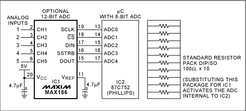
Figure 1. The connections shown enable this µC to subsistute an external 12-bit A/D converter for its internal 8-bit converter. Replacing the external converter with the resister network causes the µC to resume use of its converter.
A socket lets you plug in the external A/D converter when you need it; otherwise you plug in the network of ten 10Ω resistors. At power-up, the µC executes a routine that looks for the external converter. If present, it is used; if not, the internal 8-bit converter is used. (Internally, the chip handles all conversion results as 12-bit values.)
This idea relies on the fact that the 87C752's five A/D-input pins can also serve as the bidirectional pins of an 8051 port (port 1). The resistor network connects the internal A/D converter directly to the applied analog inputs. Or, replacing the network with the external A/D converter connects those inputs to corresponding channels on that converter, and the µC's A/D-input pins (now acting as a bidirectional port) serve as a digital interface to the converter. By fortune and design, the change from external to internal converter is effected by simple pin-for-pin jumpers across the socket.
The assembly-language software routine "looks" for the external converter by triggering a conversion and noting whether or not the converter's busy flag (SSTRB) goes low. If it does, the µC sets an internal global flag (AD12) that tells it to use its external-converter routines for each subsequent conversion. This action is transparent to the calling routine. The conversion result, returned as bytes ADHI and ADLO, has the same format in either case except the four LSBs are zero for 8-bit-converter data.
Note that the µC's full scale is 5V, but the converter shown (MAX186) sets its full-scale input range with an internal reference of 4.096V. Software resolves the incompatibility in this example. Otherwise, you can replace the MAX186 with a MAX188 (a similar device with no internal reference) plus a separate 5V reference.
* Set modem to 2400 baud, 8 data bits, no parity, and 1 stop bit. Dial (617) 558-4241 and log on. (New users must set up an account; this is free.) Type SS/DI_SIG to select the Design Ideas section, RK1554 to select this idea, and D for downloading the file. Select protocol, download the file, log off, and then "unzip" the file.
A similar article appeared in the July 7, 1994 issue of EDN magazine.
The simple circuit of Figure 1 (plus a software routine) lets you substitute a multichannel, 12-bit A/D converter for the 8-bit A/D converter internal to an 87C752 microcontroller. Thus, a single assembly can implement both the low- and high-performance versions of a system. The software mentioned can be downloaded from EDN's free electronic bulletin board service (BBS)*.

Figure 1. The connections shown enable this µC to subsistute an external 12-bit A/D converter for its internal 8-bit converter. Replacing the external converter with the resister network causes the µC to resume use of its converter.
A socket lets you plug in the external A/D converter when you need it; otherwise you plug in the network of ten 10Ω resistors. At power-up, the µC executes a routine that looks for the external converter. If present, it is used; if not, the internal 8-bit converter is used. (Internally, the chip handles all conversion results as 12-bit values.)
This idea relies on the fact that the 87C752's five A/D-input pins can also serve as the bidirectional pins of an 8051 port (port 1). The resistor network connects the internal A/D converter directly to the applied analog inputs. Or, replacing the network with the external A/D converter connects those inputs to corresponding channels on that converter, and the µC's A/D-input pins (now acting as a bidirectional port) serve as a digital interface to the converter. By fortune and design, the change from external to internal converter is effected by simple pin-for-pin jumpers across the socket.
The assembly-language software routine "looks" for the external converter by triggering a conversion and noting whether or not the converter's busy flag (SSTRB) goes low. If it does, the µC sets an internal global flag (AD12) that tells it to use its external-converter routines for each subsequent conversion. This action is transparent to the calling routine. The conversion result, returned as bytes ADHI and ADLO, has the same format in either case except the four LSBs are zero for 8-bit-converter data.
Note that the µC's full scale is 5V, but the converter shown (MAX186) sets its full-scale input range with an internal reference of 4.096V. Software resolves the incompatibility in this example. Otherwise, you can replace the MAX186 with a MAX188 (a similar device with no internal reference) plus a separate 5V reference.
* Set modem to 2400 baud, 8 data bits, no parity, and 1 stop bit. Dial (617) 558-4241 and log on. (New users must set up an account; this is free.) Type SS/DI_SIG to select the Design Ideas section, RK1554 to select this idea, and D for downloading the file. Select protocol, download the file, log off, and then "unzip" the file.
A similar article appeared in the July 7, 1994 issue of EDN magazine.
 电子发烧友App





评论