Abstract: This article explains how to interface a GPIO port to an SPI peripheral. It defines the basics of the SPI protocol, the signals and the four transfer variations for the SCK signal. A software routine is included to implement the SPI interface using the MAX7651, a flash programmable 12-bit integrated data-acquisition system.
The 4 pins of the SPI interface are as follows:
Table 1. The Four Variations
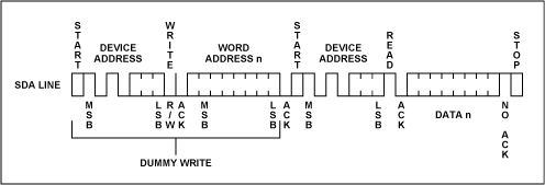
When reading a data sheet for a SPI peripheral, it is common to see a reference to the SPI mode as CPOL = 0, CPHA = 0, etc., even though the chip itself does not physically contain these bit definitions. Rather, the SPI interface is "hard-wired" to send/receive data as if the CPOL and CPHA bits had been set to 0. For example, the MAX5154 12-bit DAC uses a SPI interface with rising-edge mid-bit data transfer. This corresponds to CPOL = 0, CPHA = 0 protocol. Because this is by far the most common SPI transfer, that is the example code we will discuss. See the following diagram, which is from the MAX5154 data sheet. The signal Active-Low CS is the SPI signal Active-Low SS, SCLK is SCK, and DIN would be connected to MODI, because the peripheral is a Slave, with only an input (no readback). This part uses 16 bits in the transfer.

Figure 1. Serial interface timing diagram.
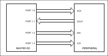
Figure 2 shows typical connections between the MAX7651/MAX7652 and an SPI peripheral.

Figure 2. General SPI connection.
The number {N} inside the comment field is the number of clock cycles to execute the instruction.
; SPI data transfer for 8-bit peripherals. MAX7651 is Master; peripheral is Slave.
;
; The following SPI-defined pins are used. (Some peripherals are write only, so only 3 wires are needed.)
; SCK: The data transfer clock
; MIS Master Input data (from peripheral), not always used
; MOSI: Master Output data (to peripheral)
; SS: Slave Select (active low)
;
;
; Now we need to use some of the internal RAM in the MAX7651 as data storage.
; For speed of execution, two of these variables must be located in the RAM area
; that allows bit addressing within the byte. In the MAX7651, the RAM space corresponds
; to addresses 20H to 2FH. Addresses below 20H or above 2FH cannot be bit-addressed!
;
; Lastly, we need a loop counter to keep track of sending the 8 bits.
; This can be either an 'R' register (R0-R7) or
; any RAM register (doesn't have to be bit-addressable). Let's use a RAM
; register.
;
; It is assumed that when called, the chip select bit SS is already set to 1.
The total number of CPU cycles to transfer 8 bits (both read and write to Slave) is 6 + 8 × 23 + 1 = 191. For reading or writing only, the total is 6 + 8 × 18 + 1 = 151 CPU cycles. The following table shows various transfer rates using common MAX7651 clock speeds.
Table 2. Transfer Rates
From this table, we can see that the fastest SPI byte transfer is approximately 15.7KHz whereas the slowest rate is 5.2KHz. This is much slower than a dedicated 1MHz SPI hardware port! Therefore, if the MAX7651 is to be used as a Slave, then the SPI Master must be set for the slowest bit transfer speed (125KHz) and the MAX7651 must operate at a 12MHz clock speed.
Introduction
The SPI™ bus is a 4-wire serial communications interface used by many microprocessor peripheral chips. The MAX7651 microprocessor does not include dedicated hardware to implement the interface. However, simple software routines are shown that can send and receive data to SPI peripherals.The 4 pins of the SPI interface are as follows:
- SCK (Serial Data Clock): Data is shifted/latched on the rising or falling edge of SCK (see next section).
- MOSI (Master Output/Slave Input): Data is transmitted out of this pin if the chip is a Master and into this pin if the chip is a Slave.
- MISO (Master Input/Slave Output): Data is receivedinto this pin if the chip is a Master and transmitted out of this pin if the chip is a Slave.
- Active-Low CS (Chip Select, active low): Tells the peripheral that a transfer is about to begin.
Table 1. The Four Variations
|
|
|
|
|
|
|
SCK transitions in middle of bit timing. |
|
|
|
SCK transitions in middle of bit timing. |
|
|
|
SCK transitions at beginning of bit timing. |
|
|
|
SCK transitions at beginning of bit timing. |
When reading a data sheet for a SPI peripheral, it is common to see a reference to the SPI mode as CPOL = 0, CPHA = 0, etc., even though the chip itself does not physically contain these bit definitions. Rather, the SPI interface is "hard-wired" to send/receive data as if the CPOL and CPHA bits had been set to 0. For example, the MAX5154 12-bit DAC uses a SPI interface with rising-edge mid-bit data transfer. This corresponds to CPOL = 0, CPHA = 0 protocol. Because this is by far the most common SPI transfer, that is the example code we will discuss. See the following diagram, which is from the MAX5154 data sheet. The signal Active-Low CS is the SPI signal Active-Low SS, SCLK is SCK, and DIN would be connected to MODI, because the peripheral is a Slave, with only an input (no readback). This part uses 16 bits in the transfer.

Figure 1. Serial interface timing diagram.
Code Example: 8-Bit Data Transfer
The following example is the most common type of SPI transfer, with CPO = 0 and CPHA = 0. The routine does not assume anything about the clock speed of the MAX7651, as the I/O port bits are simply "bit-banged" as fast as possible. Data-transfer times are shown at the end of this section.Figure 2 shows typical connections between the MAX7651/MAX7652 and an SPI peripheral.

Figure 2. General SPI connection.
The number {N} inside the comment field is the number of clock cycles to execute the instruction.
; SPI data transfer for 8-bit peripherals. MAX7651 is Master; peripheral is Slave.
;
; The following SPI-defined pins are used. (Some peripherals are write only, so only 3 wires are needed.)
; SCK: The data transfer clock
; MIS Master Input data (from peripheral), not always used
; MOSI: Master Output data (to peripheral)
; SS: Slave Select (active low)
;
| SCK | EQU | P1.0 | ||
| MISO | EQU | P1.1 | ||
| MOSI | EQU | P1.2 | ||
| CS | EQU | P1.3 | ; Use Port 1, but this is 100% arbitrary. Use any available pins. |
;
; Now we need to use some of the internal RAM in the MAX7651 as data storage.
; For speed of execution, two of these variables must be located in the RAM area
; that allows bit addressing within the byte. In the MAX7651, the RAM space corresponds
; to addresses 20H to 2FH. Addresses below 20H or above 2FH cannot be bit-addressed!
| SPI_In | EQU | 20H | ; Result of 8-bit read from Slave. | |
| SPI_Out | EQU | 21H | ; Data we wish to send to Slave. |
;
; Lastly, we need a loop counter to keep track of sending the 8 bits.
; This can be either an 'R' register (R0-R7) or
; any RAM register (doesn't have to be bit-addressable). Let's use a RAM
; register.
| LOOP | EQU | 30H | ; Can be anywhere in the map; this is just an example. |
;
; It is assumed that when called, the chip select bit SS is already set to 1.
| SPI_I | CLR | SCK | ; SCK starts off low. {1} | |
| CLR | CS | ; Clearing CS begins the data transfer. {1} | ||
| SETB | MISO | ; To be used as input, must be set internally. {1} | ||
| MOV | LOOP,#8 | ; Eight bits to transfer. {3} | ||
| XFER: | MOV | C,SPI_Out.7 | ; Move bit 7 into Carry (SPI is MSB first). {2} | |
| MOV | MOSI,C | ; I/O port reflects the Carry bit, which is the Data bit. {2} | ||
| SETB | SCK | ; Generate SCK rising edge, after Data is stable. {1} | ||
| MOV | C,MISO | ; Read data from Slave into Carry (optional). {2} | ||
| MOV | SPI_In.7,C | ; Copy into the received data byte, bit-7 position. {2} | ||
| CLR | SCK | ; Generate SCK falling edge, after data read in. {1} | ||
| MOV | A,SPI_Out | ; Accumulator is temp holder for shift operation. {2} | ||
| RL | A | ; Rotate left (but not through Carry!). {1} | ||
| MOV | SPI_Out, A | ; Prepare bit 7 for next transfer to Slave. {2} | ||
| MOV | A,SPI_In | ; Get previous Slave read data. {2} | ||
| RL | A | ; Rotate left to get next bit position into proper spot. {1} | ||
| MOV | SPI_In,A | ; Save result. {2} | ||
| DJNZ | LOOP,XFER | ; Decrement LOOP. Jump if not zero to XFER. {3} | ||
| ; Transfer done. | ||||
| SETB | CS | ; De-assert chip select. {1} | ||
| .END | ; Tell assembler code completed. | |||
The total number of CPU cycles to transfer 8 bits (both read and write to Slave) is 6 + 8 × 23 + 1 = 191. For reading or writing only, the total is 6 + 8 × 18 + 1 = 151 CPU cycles. The following table shows various transfer rates using common MAX7651 clock speeds.
Table 2. Transfer Rates
|
|
|
Transfer Time |
|
|
|
|
|
|
|
|
|
|
|
|
From this table, we can see that the fastest SPI byte transfer is approximately 15.7KHz whereas the slowest rate is 5.2KHz. This is much slower than a dedicated 1MHz SPI hardware port! Therefore, if the MAX7651 is to be used as a Slave, then the SPI Master must be set for the slowest bit transfer speed (125KHz) and the MAX7651 must operate at a 12MHz clock speed.
SPI is a trademark of Motorola, Inc.
 电子发烧友App


评论