Abstract: This article explains the architecture and operation of pipelined analog-to-digital converters (ADCs). It discusses key performance characteristics such as architecture, latency, digital error correction, component accuracy, and digital calibration. The article also briefly compares pipelines ADCs to other data converter architectures.
The pipelined analog-to-digital converter (ADC) has become the most popular ADC architecture for sampling rates from a few megasamples per second (Msps) up to 100Msps+. Resolutions range from eight bits at the faster sample rates up to 16 bits at the lower rates. These resolutions and sampling rates cover a wide range of applications, including CCD imaging, ultrasonic medical imaging, digital receivers, base stations, digital video (for example, HDTV), xDSL, cable modems, and fast Ethernet.
Applications with lower sampling rates are still the domain of the successive approximation register (SAR) and integrating architectures, and more recently, oversampling/sigma-delta ADCs. The highest sampling rates (a few hundred Msps or higher) are still obtained using flash ADCs. Nonetheless, pipelined ADCs of various forms have improved greatly in speed, resolution, dynamic performance, and low power in recent years.

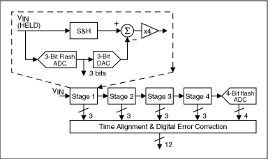
Figure 1. Pipelined ADC with four 3-bit stages (each stage resolves two bits).
In this schematic, the analog input, VIN, is first sampled and held steady by a sample-and-hold (S&H), while the flash ADC in stage one quantizes it to three bits. The 3-bit output is then fed to a 3-bit DAC (accurate to about 12 bits), and the analog output is subtracted from the input. This "residue" is then gained up by a factor of four and fed to the next stage (Stage 2). This gained-up residue continues through the pipeline, providing three bits per stage until it reaches the 4-bit flash ADC, which resolves the last 4LSB bits. Because the bits from each stage are determined at different points in time, all the bits corresponding to the same sample are time-aligned with shift registers before being fed to the digital-error-correction logic. Note when a stage finishes processing a sample, determining the bits, and passing the residue to the next stage, it can then start processing the next sample received from the sample-and-hold embedded within each stage. This pipelining action is the reason for the high throughput.
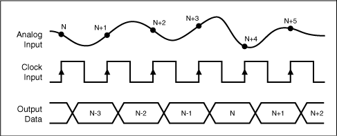
Figure 2. Data latency in a pipelined ADC.
If one of the comparators in the first 3-bit flash ADC has a significant offset when an analog input close to the trip point of this comparator is applied, then an incorrect 3-bit code and thus an incorrect 3-bit DAC output would result, thus producing a different residue. As long as this gained-up residue does not overrange the subsequent 3-bit ADC, it can be proven that the LSB code generated by the remaining pipeline (when added to the incorrect 3-bit MSB code) will give the correct ADC output code. The implication is that none of the flash ADCs in Figure 1 has to be as accurate as the entire ADC. In fact, the 3-bit flash ADCs in Stages 1 through 4 require only about four bits of accuracy.
The digital error correction will not correct for errors made in the final 4-bit flash conversion. Any error made at that conversion is suppressed by the large (44) cumulative gain preceding the 4-bit flash. Thus the final stage only needs to be more than 4-bits accurate.
Although each stage generates three raw bits in the Figure 1 example, because the interstage gain is only 4, each stage (Stages 1 to 4) effectively resolves only two bits. The extra bit is simply to reduce the size of the residue by one half, allowing extra range in the next 3-bit ADC for digital error correction, as mentioned above. This process is called "1-bit overlap" between adjacent stages. The effective number of bits of the entire ADC is therefore 2 + 2 + 2 + 2 + 4 = 12 bits.
In most pipelined ADCs designed with CMOS or BiCMOS technology, the S&H, DAC, summation node, and gain amplifier are usually implemented as a single switched-capacitor circuit block called a multiplying DAC (MDAC). The major factor limiting MDAC accuracy is the inherent capacitor mismatch. A purely bipolar implementation would be more complicated and would suffer mainly from resistor mismatch in the current-source DAC and the interstage gain amplifier.
In general, for about 12 bits of accuracy or higher, some form of capacitor/resistor trimming or digital calibration is required, especially for the first two stages.
Calibration starts from the MDAC in the third stage; beyond the third stage the MDAC error terms are small enough that calibration is not needed. The third-stage output is digitized by the remaining pipelined ADC, and the error terms are stored in on-chip RAM. Once the third MDAC is calibrated, it can be used to calibrate the second MDAC in a similar fashion. Likewise, once the second and third MDAC are calibrated, they are used to calibrate the first MDAC. Averaging is used (especially in the first and second MDAC) to ensure that the calibration is noise-free. During normal conversions, those error terms are recalled from the RAM and used to adjust the outputs from the digital-error-correction logic.

Figure 3. MAX1200 pipelined ADC architecture.
The CMOS MAX1425 (10-bit, 20Msps) and the MAX1426 (10-bit, 10Msps) family uses the popular 1.5-bit-per-stage architecture; each stage resolves one bit with 0.5-bit overlap. Each 1.5-bit stage has a 1.5-bit flash ADC (only two comparators), versus a full 2-bit flash ADC. It can be shown that, with digital error correction, this works the same way as a regular MDAC stage with 2-bit flash ADC and DAC. These converters achieve a high SNR of 59dB with 10MHz analog inputs sampled at 20Msps.
The MAX1444/MAX1446/MAX1448/MAX1449 family (10-bit, 40/60/80/105Msps, respectively) is the latest generation of high-speed, very-low-power, 10-bit ADCs employing the 1.5-bit-per-stage architecture. These CMOS devices incorporate wideband low-distortion, track-and-hold amplifiers to ensure excellent dynamic performance throughout and beyond the Nyquist band. Undersampling, popular in digital receiver design, is possible with these ADC families.
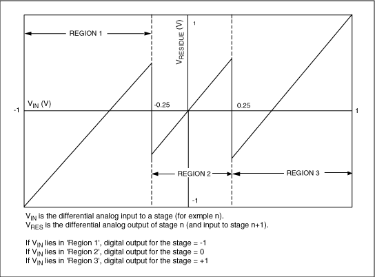
Figure 4. VRESIDUE vs. VIN transfer characteristics.
A 1.5-bit flash ADC (two comparators) compares the analog input to the comparator thresholds, which are -0.25V and +0.25V in this example. The ADC then gives a digital output corresponding to the region in which the analog input falls. The 1.5-bit indicates that there are three regions on the VRESIDUE vs. VIN transfer characteristics. A 1-bit ADC would have two regions (1/High or 0/Low) and a 2-bit ADC would have four regions (00, 01, 10, and 11) on the transfer characteristics.
Depending on the region in which the input to the flash ADC falls, the residue voltage is calculated as follows and is fed to the next stage as the input voltage.

Table 1 illustrates an example of how a sampled +0.6 analog input voltage is converted to a digital output in a 7-stage pipelined ADC. The first stage of the pipelined ADC is responsible for the most significant bit, and the seventh stage gives the least significant bit of the digital output.
Table 1. 7-Bit Pipelined ADC with +0.6V Analog Input Converts to a Digital Output
Using the digital output of each stage and its decimal place value, the sampled +0.6V analog input voltage would correspond t
[(64 × 1) + (32 × 0) + (16 × 1) + (8 × 0) + (4 × -1) + (2 × 0) + (1 × 1)] = 77
A digital output of 127 (all 1s) will correspond to analog input of 1V. Therefore, a digital output of 77 will correspond to 77/127 = 0.606V, which is a good approximation of the sampled analog input applied to the pipelined ADC.
A pipelined ADC, however, generally requires significantly more silicon area than an equivalent SAR. A SAR also displays a latency of only one cycle (one cycle = 1/Fsample), versus about three or more cycles in a typical pipeline ADC. As with a pipeline, a SAR with more than 12 bits of accuracy usually requires some form of trimming or calibration.
Extremely fast 8-bit flash ADCs (or their folding/interpolation variants) do exist with sampling rates as high as 1.5Gsps (for example, the MAX104/MAX106/MAX108). It is much harder to find a 10-bit flash, while 12-bit (or above) flash ADCs are not commercially viable products. This is simply because in a flash ADC the number of comparators increases by a factor of 2 for every extra bit of resolution; simultaneously, each comparator must be twice as accurate. In a pipeline, however, to a first order the complexity only increases linearly, not exponentially, with the resolution.
At sampling rates obtainable by both pipeline and flash converters, a pipelined device usually has much lower power consumption than a flash. A pipeline ADC is typically less susceptible to comparator metastability. Comparator metastability in a flash can lead to sparkle-code errors, a condition in which the ADC provides unpredictable, erratic conversion results.
Sigma-delta converters trade speed for resolution. The need to sample many times (for example, at least 16 times, but often much higher) to produce one final sample causes the internal analog components in the sigma-delta modulator to operate much faster than the final data rate. The digital decimation filter is also nontrivial to design, and consumes a lot of silicon area. The fastest, high-resolution sigma-delta-type converters are not expected to have more than a few MHz of bandwidth in the near future. Like pipelined ADCs, sigma-delta converters also have latency.
¹For more details, please refer to the application note, "Pipeline ADCs Come of Age".
The pipelined analog-to-digital converter (ADC) has become the most popular ADC architecture for sampling rates from a few megasamples per second (Msps) up to 100Msps+. Resolutions range from eight bits at the faster sample rates up to 16 bits at the lower rates. These resolutions and sampling rates cover a wide range of applications, including CCD imaging, ultrasonic medical imaging, digital receivers, base stations, digital video (for example, HDTV), xDSL, cable modems, and fast Ethernet.
Applications with lower sampling rates are still the domain of the successive approximation register (SAR) and integrating architectures, and more recently, oversampling/sigma-delta ADCs. The highest sampling rates (a few hundred Msps or higher) are still obtained using flash ADCs. Nonetheless, pipelined ADCs of various forms have improved greatly in speed, resolution, dynamic performance, and low power in recent years.
Pipelined ADC Architecture
Figure 1 shows a block diagram of a 12-bit pipelined ADC.
Figure 1. Pipelined ADC with four 3-bit stages (each stage resolves two bits).
In this schematic, the analog input, VIN, is first sampled and held steady by a sample-and-hold (S&H), while the flash ADC in stage one quantizes it to three bits. The 3-bit output is then fed to a 3-bit DAC (accurate to about 12 bits), and the analog output is subtracted from the input. This "residue" is then gained up by a factor of four and fed to the next stage (Stage 2). This gained-up residue continues through the pipeline, providing three bits per stage until it reaches the 4-bit flash ADC, which resolves the last 4LSB bits. Because the bits from each stage are determined at different points in time, all the bits corresponding to the same sample are time-aligned with shift registers before being fed to the digital-error-correction logic. Note when a stage finishes processing a sample, determining the bits, and passing the residue to the next stage, it can then start processing the next sample received from the sample-and-hold embedded within each stage. This pipelining action is the reason for the high throughput.
Data Latency
Because each sample must propagate through the entire pipeline before all its associated bits are available for combining in the digital-error-correction logic, data latency is associated with pipelined ADCs. In the example in Figure 1, this latency is about three cycles (see Figure 2).
Figure 2. Data latency in a pipelined ADC.
Digital Error Correction
Most modern pipelined ADCs employ a technique called "digital error correction" to greatly reduce the accuracy requirement of the flash ADCs (and thus the individual comparators). In Figure 1, notice that the 3-bit residue at the summation-node output has a dynamic range one-eighth that of the original Stage 1 input (VIN), yet the subsequent gain is only 4. Therefore, the input to Stage 2 occupies only half the range of the 3-bit ADC in Stage 2 (that is, when there is no error in the first 3-bit conversion in Stage 1).If one of the comparators in the first 3-bit flash ADC has a significant offset when an analog input close to the trip point of this comparator is applied, then an incorrect 3-bit code and thus an incorrect 3-bit DAC output would result, thus producing a different residue. As long as this gained-up residue does not overrange the subsequent 3-bit ADC, it can be proven that the LSB code generated by the remaining pipeline (when added to the incorrect 3-bit MSB code) will give the correct ADC output code. The implication is that none of the flash ADCs in Figure 1 has to be as accurate as the entire ADC. In fact, the 3-bit flash ADCs in Stages 1 through 4 require only about four bits of accuracy.
The digital error correction will not correct for errors made in the final 4-bit flash conversion. Any error made at that conversion is suppressed by the large (44) cumulative gain preceding the 4-bit flash. Thus the final stage only needs to be more than 4-bits accurate.
Although each stage generates three raw bits in the Figure 1 example, because the interstage gain is only 4, each stage (Stages 1 to 4) effectively resolves only two bits. The extra bit is simply to reduce the size of the residue by one half, allowing extra range in the next 3-bit ADC for digital error correction, as mentioned above. This process is called "1-bit overlap" between adjacent stages. The effective number of bits of the entire ADC is therefore 2 + 2 + 2 + 2 + 4 = 12 bits.
Component Accuracy
Digital error correction does not correct gain or linearity errors in the individual DAC and gain amplifiers. The front-end S&Hs and DAC actually need about 12-bit accuracy, whereas the components in subsequent stages require less accuracy (for example, 10-bit accuracy for Stage 2, 8-bit for Stage 3, and so forth). This need for reduced accuracy is because the later stages’ error terms are divided down by the preceding interstage gain(s). This fact is often exploited to save additional power by making the pipelined stages progressively smaller.In most pipelined ADCs designed with CMOS or BiCMOS technology, the S&H, DAC, summation node, and gain amplifier are usually implemented as a single switched-capacitor circuit block called a multiplying DAC (MDAC). The major factor limiting MDAC accuracy is the inherent capacitor mismatch. A purely bipolar implementation would be more complicated and would suffer mainly from resistor mismatch in the current-source DAC and the interstage gain amplifier.
In general, for about 12 bits of accuracy or higher, some form of capacitor/resistor trimming or digital calibration is required, especially for the first two stages.
Digital Calibration
The MAX1200 (16-bit, 1Msps), MAX1201 (14-bit 2Msps), and MAX1205 (14-bit, 1Msps) family¹ of ADCs employs digital calibration to ensure excellent accuracy and dynamic performance. Each device is a CMOS pipelined ADC with four 4-bit stages (with 1-bit overlap) and a 5-bit flash ADC at the end, giving a total of 3 + 3 + 3 + 3 + 5 = 17 raw bits (see Figure 3). The extra one to three bits are required by the digital calibration to quantize the error terms to greater accuracy than the ADC itself; the extra bits are also discarded to give either 14 bits or 16 bits overall.Calibration starts from the MDAC in the third stage; beyond the third stage the MDAC error terms are small enough that calibration is not needed. The third-stage output is digitized by the remaining pipelined ADC, and the error terms are stored in on-chip RAM. Once the third MDAC is calibrated, it can be used to calibrate the second MDAC in a similar fashion. Likewise, once the second and third MDAC are calibrated, they are used to calibrate the first MDAC. Averaging is used (especially in the first and second MDAC) to ensure that the calibration is noise-free. During normal conversions, those error terms are recalled from the RAM and used to adjust the outputs from the digital-error-correction logic.

Figure 3. MAX1200 pipelined ADC architecture.
Different Variations
The example in Figure 1 shows that there can be many variations of pipelined ADCs, depending, that is, on several variables: how many bits each stage resolves; the number of bits in the LSB flash ADC; and whether digital calibration or trimming is used to improve the accuracy of the first couple of stages. This partition of bits per stage is determined in part by the target sampling rate and resolution. In general, higher speed CMOS pipelined ADCs tend to favor a lower number of bits per stage (as low as just one bit per stage so that the interstage gain is only 2), because it is difficult to realize wideband amplifiers of very high gain in CMOS. Lower sampling-rate CMOS pipelined ADCs and bipolar pipelined ADCs (even those with a very high sampling rate) tend to favor more bits per stage. This also results in less data latency.The CMOS MAX1425 (10-bit, 20Msps) and the MAX1426 (10-bit, 10Msps) family uses the popular 1.5-bit-per-stage architecture; each stage resolves one bit with 0.5-bit overlap. Each 1.5-bit stage has a 1.5-bit flash ADC (only two comparators), versus a full 2-bit flash ADC. It can be shown that, with digital error correction, this works the same way as a regular MDAC stage with 2-bit flash ADC and DAC. These converters achieve a high SNR of 59dB with 10MHz analog inputs sampled at 20Msps.
The MAX1444/MAX1446/MAX1448/MAX1449 family (10-bit, 40/60/80/105Msps, respectively) is the latest generation of high-speed, very-low-power, 10-bit ADCs employing the 1.5-bit-per-stage architecture. These CMOS devices incorporate wideband low-distortion, track-and-hold amplifiers to ensure excellent dynamic performance throughout and beyond the Nyquist band. Undersampling, popular in digital receiver design, is possible with these ADC families.
A 1.5-Bit-Per-Stage Pipelined ADC

Figure 4. VRESIDUE vs. VIN transfer characteristics.
A 1.5-bit flash ADC (two comparators) compares the analog input to the comparator thresholds, which are -0.25V and +0.25V in this example. The ADC then gives a digital output corresponding to the region in which the analog input falls. The 1.5-bit indicates that there are three regions on the VRESIDUE vs. VIN transfer characteristics. A 1-bit ADC would have two regions (1/High or 0/Low) and a 2-bit ADC would have four regions (00, 01, 10, and 11) on the transfer characteristics.
Depending on the region in which the input to the flash ADC falls, the residue voltage is calculated as follows and is fed to the next stage as the input voltage.

Table 1 illustrates an example of how a sampled +0.6 analog input voltage is converted to a digital output in a 7-stage pipelined ADC. The first stage of the pipelined ADC is responsible for the most significant bit, and the seventh stage gives the least significant bit of the digital output.
Table 1. 7-Bit Pipelined ADC with +0.6V Analog Input Converts to a Digital Output
| Stage | VIN (V) | Region on the VRESIDUE vs. VIN Transfer Characteristic (See Figure 4) |
Digital Output (-1 , 0, or +1) | Decimal Place Value | VRESIDUE (VIN for the Next Stage) |
| 1 | 0.6 | Region 3 | +1 | 64 | 2 × 0.6 - 1 |
| 2 | 0.2 | Region 2 | 0 | 32 | 2 × 0.2 |
| 3 | 0.4 | Region 3 | +1 | 16 | 2 × 0.4 - 1 |
| 4 | -0.2 | Region 2 | 0 | 8 | 2 × (-0.2) |
| 5 | -0.4 | Region 1 | -1 | 4 | 2 × (-0.4) + 1 |
| 6 | 0.2 | Region 2 | 0 | 2 | 2 × 0.2 |
| 7 | 0.4 | Region 3 | 1 | 1 | Not required |
Using the digital output of each stage and its decimal place value, the sampled +0.6V analog input voltage would correspond t
[(64 × 1) + (32 × 0) + (16 × 1) + (8 × 0) + (4 × -1) + (2 × 0) + (1 × 1)] = 77
A digital output of 127 (all 1s) will correspond to analog input of 1V. Therefore, a digital output of 77 will correspond to 77/127 = 0.606V, which is a good approximation of the sampled analog input applied to the pipelined ADC.
Pipelined ADC versus Other ADCs
Versus SAR
In a successive approximation register (SAR) ADC, the bits are decided by a single high-speed, high-accuracy comparator bit by bit, from the MSB down to the LSB. The SAR ADC compares the analog input with a DAC, whose output is updated by previously decided bits and successively approximates the analog input. This serial nature of SAR limits its operating speed to no more than a few Msps, and still slower for very high resolutions (14 to 16 bits). A pipelined ADC, however, employs a parallel structure in which each stage works on 1 to a few bits (of successive samples) concurrently. Although there is only one comparator in a SAR, this comparator must be fast (clocked at approximately the number of bits x the sample rate) and as accurate as the ADC itself. In contrast, none of the comparators inside a pipelined ADC needs this degree of speed or accuracy.A pipelined ADC, however, generally requires significantly more silicon area than an equivalent SAR. A SAR also displays a latency of only one cycle (one cycle = 1/Fsample), versus about three or more cycles in a typical pipeline ADC. As with a pipeline, a SAR with more than 12 bits of accuracy usually requires some form of trimming or calibration.
Versus Flash
Despite the inherent parallelism, a pipelined ADC still requires accurate analog amplification in DACs and interstage gain amplifiers, and thus significant linear settling time. A purely flash ADC, however, has a large bank of comparators, each consisting of wideband, low-gain preamps followed by a latch. The preamps, unlike those amplifiers in a pipelined ADC, must provide gains that do not need to be linear or accurate; only the comparators' trip points must be accurate. As a result, a pipelined ADC cannot match the speed of a well-designed flash ADC.Extremely fast 8-bit flash ADCs (or their folding/interpolation variants) do exist with sampling rates as high as 1.5Gsps (for example, the MAX104/MAX106/MAX108). It is much harder to find a 10-bit flash, while 12-bit (or above) flash ADCs are not commercially viable products. This is simply because in a flash ADC the number of comparators increases by a factor of 2 for every extra bit of resolution; simultaneously, each comparator must be twice as accurate. In a pipeline, however, to a first order the complexity only increases linearly, not exponentially, with the resolution.
At sampling rates obtainable by both pipeline and flash converters, a pipelined device usually has much lower power consumption than a flash. A pipeline ADC is typically less susceptible to comparator metastability. Comparator metastability in a flash can lead to sparkle-code errors, a condition in which the ADC provides unpredictable, erratic conversion results.
Versus the Sigma-Delta Converter
Traditionally, oversampling/sigma-delta-type converters commonly used in digital audio have a limited bandwidth of about 22kHz. Recently some high-bandwidth sigma-delta converters reached a bandwidth of 1MHz to 2MHz with 12 to 16 bits of resolution. These specifications indicate very high-order sigma-delta modulators (for example, fourth or even higher) incorporating a multi-bit ADC and multi-bit feedback DAC. Their main applications are in ADSL. A sigma-delta converter needs no special trimming/calibration, even for 16 to 18 bits of resolution. They also require no steep rolling-off anti-alias filter at the analog inputs, because the sampling rate is much higher than the effective bandwidth. The backend digital filters take care of that task. The oversampling nature of the sigma-delta converter also tends to "average out" any system noise at the analog inputs.Sigma-delta converters trade speed for resolution. The need to sample many times (for example, at least 16 times, but often much higher) to produce one final sample causes the internal analog components in the sigma-delta modulator to operate much faster than the final data rate. The digital decimation filter is also nontrivial to design, and consumes a lot of silicon area. The fastest, high-resolution sigma-delta-type converters are not expected to have more than a few MHz of bandwidth in the near future. Like pipelined ADCs, sigma-delta converters also have latency.
Versus Half- (Two-Step) Flash
A two-step flash converter can be generalized as a two-stage pipeline device. As the number of bits increases (for example, 12 bits or higher) with digital error correction, however, each stage would need to incorporate a 6- to 7-bit flash ADC. The interstage gain amplifier would also need very high gain. Therefore, for higher resolution, it is wiser to use more than two stages.Conclusion
The pipelined ADC is the architecture of choice for sampling rates from a few Msps up to 100Msps+. Design complexity increases only linearly (not exponentially) with the number of bits, thus providing converters with high speed, high resolution, and low power at the same time. Pipelined ADCs are very useful for a wide range of applications, most notably in digital communication where a converter's dynamic performance is often more important than traditional DC specifications like differential nonlinearity (DNL) and integral nonlinearity (INL). The data latency of pipelined ADCs is of little concern in most applications. Maxim continually develops new converters for its portfolio of pipelined ADCs. These pipelined ADCs nicely complement its ADC families designed with other architectures.¹For more details, please refer to the application note, "Pipeline ADCs Come of Age".
 电子发烧友App






评论