Current trends, though, are in the other direction—designers who must implement A/D conversion usually specify a packaged A/D converter (ADC) for the job. Most engineers are not aware of an alternative, and the price/performance ratios for ADCs are falling all the time. Yet, an analog comparator plus D/A converter (DAC), along with digital processing capability, form the core of a successive-approximation ADC.
The discrete comparator/DAC approach is already common in certain fields. Automatic test equipment, nuclear pulse-height discriminators, and automated time-domain reflectometers often use the technique whereby one comparator input is driven by the DAC, and the other is driven by the signal to be monitored. Following is a selection of general measurement problems and specific applications in which a comparator/DAC combination is actually more appropriate than an off-the-shelf ADC.
Transient Voltage Analysis
A brute-force technique for capturing fast-changing amplitude events (transients) is simply to digitize them with a high-speed ADC supported by a processor and fast RAM (Figure 1). Single-shot events may compel the use of this approach, as may the need to discern fine detail in the transients. Otherwise, if the transients are repetitive, you can measure their peak amplitude and other features with the DAC/comparator approach (Figure 2).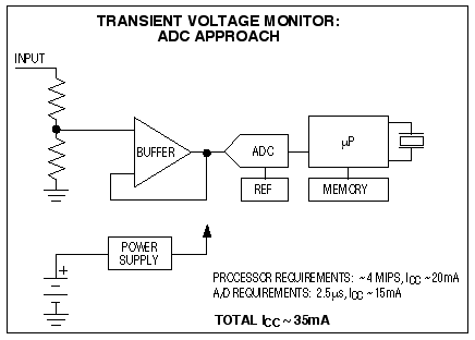
Figure 1. As the brute-force approach to transient analysis, an ADC circuit is power-hungry and expensive.
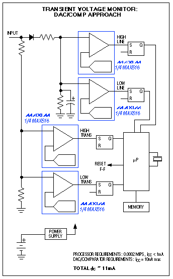
Figure 2. If the Figure 1 application can accept an iterative approach to the amplitude measurements, replacing the ADC with DAC/comparator combinations saves power and cost.
The DAC sets a trial level at one input of the comparator while the transient signal is applied to the other input. You then determine peak transient amplitudes by adjusting the DAC output, using a digital latch to capture the comparator's output response when its threshold is exceeded. Only the comparator input need sustain the full bandwidth of the transient, and the DAC output can exhibit arbitrarily long settling times without affecting the measurement accuracy. Thus, sensing in the analog domain lets you replace an expensive ADC with a low- cost DAC and comparator.
A related problem is monitoring an analog voltage with respect to tolerance limits. Many self-diagnostic instruments monitor system voltages, temperatures, and other analog quantities against limit values set in software. However, if the comparisons are made by a comparator whose setpoint value is provided by a DAC, you can reduce the processor's overhead because it need only read a single bit representing the out-of-limit condition.
This technique (analog-domain comparison) is just as accurate as the ADC technique (digital-domain comparison), so why digitize the whole value when you can simply compare it against a setpoint? One case should be mentioned: If the value must be compared against several setpoints, such as a low and high warning level and a low and high shutdown level, an ADC may be preferable to the four DACs and four comparators otherwise required.
Derive a Simple ADC from an Existing DAC
In portable instruments constrained by cost and size, an existing DAC can sometimes be persuaded to perform A/D conversions as well. Cellular phones and medical electronics, for example, often include a DAC for adjusting the contrast voltage in an LCD (Figure 3). In some cases you can also monitor a temperature or battery voltage (as described above) simply by adding a comparator and switches. The existing DAC then does double duty, with the display blanked while the DAC participates in analog-to-digital conversions. As an alternative to blanking, a simple sample/hold consisting of an analog switch and capacitor (Figure 4) can maintain the LCD contrast voltage during an A/D conversion.
Figure 3. This circuitry is commonly found in portable instruments.

Figure 4. Adding two comparators to the circuit of Figure 3 enables the DAC to double as an ADC, saving cost.
Another alternative is to substitute a low-cost dual DAC for the existing single DAC. One half of the dual DAC produces a full-time LCD-contrast voltage, while the other half helps form a full-time ADC. Whether single or dual, the DAC and comparator require support from a fast, simple software routine that drives the DAC and samples the comparator to implement successive approximation (see sidebar, Successive Approximation).
Design considerations
Combining a DAC and comparator is simple. A signal is applied to the comparator's noninverting input, and the DAC provides a digitally programmable threshold at the inverting input. The comparator then produces a logic-high output whenever the signal is more positive than its threshold. But, you must apply care in several areas.To ensure accurate threshold levels, the DAC's dc output resistance should be low with respect the the comparator's input bias current and scaling network. This concern arises mainly in very low-power circuits, for which the DAC's output resistance can be as high as 10kΩ.
Another DAC requirement is low ac output impedance. Otherwise, the comparator output's fast digital slew rate can couple through parasitic layout capacitance, producing input transients that degrade accuracy by causing oscillation. If some settling time can be sacrificed, you can lower the DAC's ac output impedance by adding a bypass capacitor at the comparator input. Instability and oscillation can result from too much capacitive load on the DAC's output amplifier, but that problem is easily fixed by adding a resistor in series with the DAC output.
The main issue for comparators is hysteresis. Most comparator circuits include hysteresis to prevent noise and oscillation, but hysteresis should be used sparingly—it also causes the threshold value to change with output state. That behavior is acceptable if the system can compensate for state-dependent hysteresis; otherwise hysteresis should be avoided.
If the comparator to be used has internal hysteresis that cannot be disabled, you can eliminate any negative effect by ensuring that the DAC output always approaches the comparator threshold from the same direction. That action is easily established by setting the DAC to zero after each bit test; i.e., by adding one line to the pseudo-code listing at the end of this article (see sidebar, Successive Approximation).
As another option, you can often eliminate the need for hysteresis by adding a small amount of capacitive feedback, which provides speedup in the comparator's linear-transition region. Or, you can add an output flip-flop or latch to capture the comparator's output state at a given instant of time.
Modern comparators are better able to handle input signals that have a limited slew rate. The MAX913 and MAX912 from Maxim, for example, are particularly effective in this respect because they are actually stable in their linear regions. Figure 5 illustrates the MAX913's performance in a high-speed, 12-bit application. As another DAC/comparator example, the Figure 6 circuit (an ultra-low-power 8-bit converter) conserves power by turning itself off when not in use.
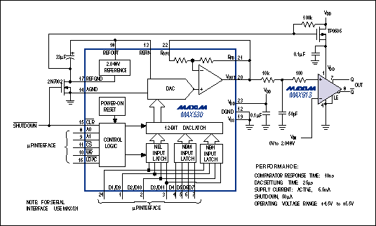
Figure 5. Because the comparator is stable in its linear region, this high-speed, 12-bit amplitude digitizer can handle slow-moving input voltages without oscillation.
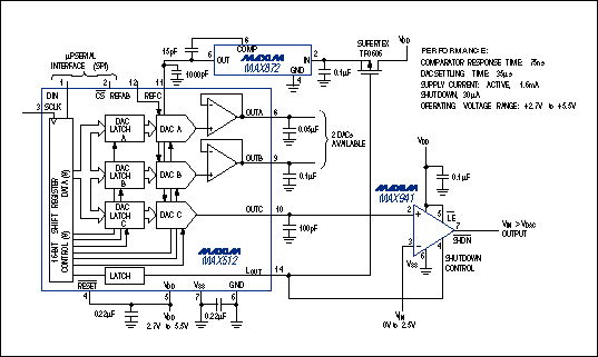
Figure 6. This low-voltage, 8-bit digitizer offers several advantages over the ADC alternative: low cost, low power consumption, and between-sample shutdown capability.
DAC/Comparator Combo ICs
Maxim offers three monolithic devices that greatly simplify a design by combining the functions of a comparator and a DAC. Each device is suitable for the applications in this article, as well as many others.The MAX516, for example, is a quad device with sub-microsecond speed, suitable for many medium-speed, multiple-channel applications (Figure S1a).
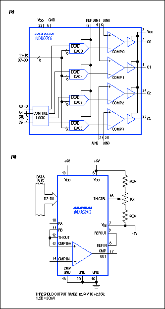
Figure S1. 8-bit DAC/comparator ICs from Maxim include the quad MAX516 (a), the high-speed, TTL-compatible MAX910 (b), and the ECL-compatible MAX911 (not shown).
The MAX910 is a single, high-speed, TTL-output DAC/comparator with 8ns propagation delay (Figure S1b). A similar device (the MAX911) is even faster-it has complementary-ECL outputs and a propagation delay of 4ns.
Successive Approximation
Successive approximation is easily illustrated by the procedure that uses a balance and a set of binary trial weights (a series of weights whose relative values are 1, 2, 4, 8, 16, etc.) to determine an object's weight. To determine the unknown weight by the quickest method (successive approximation), first balance the unknown against the largest trial weight. According to the balance indication, either remove that weight or add the next largest, and continue that process down to the smallest trial weight. The resulting best estimate of the object's weight is the sum of trial weights remaining in the balance pan.In successive-approximation ADCs, the bits of the internal DAC are analogous to the set of binary weights, and the comparator output is analogous to the balance indication. Logic for driving the bit-trial procedure can reside either in the successive-approximation register (SAR) of a packaged ADC, or in a software routine associated with the processor that controls a DAC/comparator circuit. The "pseudo-code" shown in Table S1 represents such a routine. For most processors, this routine can be realized with fewer than 20 lines of code.
Table S1. Pseudo-Code for Successive Approximation

Applications
This section presents a number of situations in which a DAC/comparator approach offers advantages over the ADC approach. The application circuits discussed are neither unusual nor esoteric, but address common problems that arise frequently.First, consider the need for a low-cost method to detect and log the sags, surges, and transients that occur on a power line. An ideal design would be a wall-cube device that detects power-line abnormalities and logs the time of each occurrence to RAM. (Sags and surges can last from milliseconds to hours; transients are as short as 10 microseconds.) The monitor must log the duration of complete failures in line power, so the monitor power should come from a battery.
The conventional solution to this problem is a controller and ADC converter. As the converter continually samples the line voltage, the controller compares each value to user-settable limits stored in software, and logs any out-of-spec condition to RAM. Because the system must be capable of tracking transients as brief as 10µs, the ADC sample interval must be considerably shorter—perhaps 2.5µs maximum as a conservative estimate. The controller must therefore process the samples at 1/2.5µs = 400ksps.
If software comparisons can be coded efficiently and the ADC requires no processor intervention, this system can operate with as few as ten instructions per sample, requiring processor performance in the 4 MIPS range. Such performance is substantial, and is not readily compatible with battery operation (Figure 1). You might then consider an analog method that responds to the derivative of an input transient instead of tracking it, but that approach appears untenable.
The alternate DAC/comparator approach in this case offers several significant advantages. It requires four DACs and four comparators (or a single MAX516), followed by a quad set/reset flip-flop. One DAC/comparator/FF combination monitors high transients, one monitors low transients, one is for sags, and one is for surges (Figure 2). Transient voltages couple directly to the comparators, but the input to the sag and surge comparators is first rectified and filtered to obtain the average value of line voltage. Appropriate rms adjustments can be made in software.
The system operates by sampling and resetting the flip-flops every T seconds, where T is the time resolution required in the transient log (perhaps 60 seconds). DACs for the high and low transient levels are set to the desired high and low threshold values. The sag and surge DACs are adjusted after each T-second interval, using a successive-approximation technique to generate high-line and low-line limits that track the current average value.
Assuming a very conservative 1000-instruction routine to perform this successive approximation and the other housekeeping chores, the average CPU performance for T = 60s is 17 instructions per second. The resulting execution rate is 0.00002 MIPS—quite suitable for low-power systems, and far below the 4 MIPS required with an ADC approach. For further power savings the controller can "sleep" most of the time, waking only to process an abnormal line condition. The circuit thus reduces power, complexity, and cost by offloading the voltage comparison from software to analog hardware.
Low-maintenance Fault Detection and Diagnostics
Printer-head control, carriage control, and many other electromechanical applications monitor critical internal voltages and temperatures to determine when to modify their operating mode. In extreme cases, this feedback enables the system to avoid self-destruction by shutting down altogether. For example, a stepper-motor controller must adjust gate drive to the output MOSFETs when necessary to avoid the excessive power dissipation associated with linear operation.Again, the conventional solution to these monitoring problems is an ADC (Figure 7a). The processor directs the ADC to make periodic measurements consistent with the time constant of the process under control. It then scales the resulting digitized values and compares them with limits in software. If they go out of bounds, it can trigger corrective action or shut down the system completely.
An alternate approach uses the DAC/comparator combination (Figure 7b). The static DAC output establishes a shutdown limit or trip value for the comparator. When a temperature change causes the comparator to trip, the comparator sends an interrupt to the processor that initiates corrective action. If necessary, the processor can also determine the absolute temperature value by initiating a software-based successive-approximation routine.
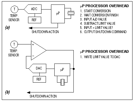
Figure 7. In this case, replacing an ADC (a) with a DAC and comparator (b) lowers system cost, response time, and software overhead.
On the other hand, to support an ADC the processor must poll the ADC, input the sample value, and compare it with the setpoint before jumping to the shutdown routine. Thus, a DAC/comparator not only saves cost and offers a quicker response than does an ADC; it also reduces the processor overhead.
Time-domain reflectometry
Finally, the low cost and low power dissipation of DAC/comparator combinations (vs. ADCs) has made practical the portable time-domain reflectometer (TDR)—an instrument that detects cable discontinuities and measures the intervening transmission length. Portable, inexpensive TDRs have become popular with the proliferation of network cabling.A TDR operates like radar; it sends a brief pulse along the line and detects any echo returned by an open, short, or other abrupt discontinuity in the line impedance. The time interval for propagation of the outward-bound pulse and its returning reflection is about 3.3ns per foot, assuming a line propagation of 0.6c (six tenths the speed of light). Thus, a 10ns timing resolution in the electronics gives a resolution in distance to the discontinuity of approximately 3 feet.
The ratio of received-pulse amplitude to transmitted-pulse amplitude is used to compute the reflection coefficient. Knowing the reflection coefficient and cable impedance you can compute the impedance of the discontinuity, and from that information deduce the nature of the discontinuity. Coaxial cables introduce a complication by attenuating the pulse on its return trip, so the software must compensate for this effect by applying an amplitude correction based on the distance measurement.
An ADC in this application would have to convert every 5ns (200Msps). Though available, such ADCs are expensive, power hungry, and generally unsuitable for portable applications.
The analog front end of an actual hand-held TDR (Figure 8) serves to illustrate the ideas described above. Digital circuitry is excluded for clarity. Though simple and without exotic components, this circuit has impressive performance. It measures termination impedance reliably and with 5% accuracy for cable lengths to 500 feet. For open or shorted terminations, it measures distances to 2000 feet. And best of all, the system (including display and digital circuitry) can operate for 20 hours on a 9V alkaline battery.
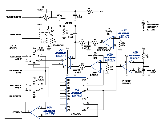
Figure 8. This circuit-the analog section of a time-domain reflectometer-relies on a DAC/comparator in place of an ADC.
The comparator in Figure 8 (IC3) provides single-supply operation with ground sensing and a propagation delay of just 10ns. The DAC (IC4) is a dual device in which one side helps with the pulse-height measurement and the other drives the LCD contrast control (as in Figure 3). Note that the DACs are driven backwards; the (normal) current outputs are driven together by a buffered reference, and the (normal) reference inputs serve as voltage outputs (each buffered by an external op amp).
A simple glitch-monostable circuit (not shown) drives the base of Q1, which in turn drives the cable with positive, 10ns-duration pulses. Any reflections from the line are coupled to the comparator via C3.
IC5 is a bandgap reference whose 1.2V output is buffered by op amp IC2d to provide a reference voltage for the dual DACs in IC4. This reference voltage is also doubled by the gain-of-2 amplifier IC2c to provide a 2.5V dc level at the comparator's noninverting input. DAC A applies 0V to 3.8V at the comparator's inverting input. Levels above 2.5V enable the determination of positive-going pulse heights, and levels below 2.5V determine the amplitude of negative-going pulses.
Each pulse entering the transmission line also enters a variable delay line in the digital circuitry, which consists of a string of 20ns delay elements controlled by a counter. This delayed pulse from the digital section jointly drives the D inputs of two flip-flops (IC1a and IC1b), which in turn are clocked by complementary TTL outputs from the comparator. Thus, time measurements amount to a race between the return pulse and the pulse going through the delay line: if the D input arrives before a clock transition the flip-flop output is high; otherwise it is zero.
To measure, set the DAC output to a low absolute level and iteratively adjust the delay until the flip-flop output remains at zero, then read the counter. Similarly, to measure the height of return pulses, iteratively adjust the DAC output until the flip-flop output remains at zero, then read the DAC. Note that two flip-flops are required to capture the comparator's leading edge for both positive and negative pulses. This leading edge rises for positive pulses and falls for negative pulses; if both were applied to a single flip-flop, the pulse width would become an unwanted part of the delay.
References
- Edward Jordan, Reference Data for Engineers, 7th Edition, (Howard Sams, 1989).
- Brian Kenner and John Wettroth, The Design of a Time-Domain Reflectometer, (Computer Applications Journal #29, October/November 1992).
- Paul Horowitz and Winfield Hill, The Art of Electronics, 2nd Edition, (Cambridge University Press, 1989).
 电子发烧友App








评论