Abstract: In any on-screen video display system or character generator, it is desirable to provide smooth transitions when changing the displayed information. Applications which display the time and date need to be updated between frames, for an unambiguous record. The MAX4455 arbitrary graphics on-screen display generator is capable of achieving these goals but designers need to account for the transfer of large amounts of data that can occur when programming many pixels. This article offers ways to make sure that your MAX4455-based OSD system will have the optimum graphics update rate.
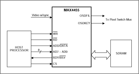
Figure 1. MAX4455 key interface signals.
Graphics data to be displayed is contained in the SDRAM memory. The organization of the data for the eight channels is via logical blocks of 512 by 1024 by 4 for each channel for a total of 2Mbits per channel and a total of 16Mbits for all eight channels. The visible pixels on the display map into memory differently for NTSC versus PAL video formats. For NTSC, 484 bits out of the 512 bits in one dimension are used to represent the 484 visible video horizontal scan lines and 712 bits out of 1024 in the other dimension are used to represent the total visible horizontal pixels per line. For the PAL format, all 512 bits are used to represent 512 video horizontal scan lines with the same 712 visible horizontal pixels per line resolution as in NTSC. In both formats, each pixel has a 4-bit resolution to represent brightness.
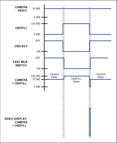
The interface between the SDRAM memory and the host processor is via the MAX4455. Data intended for the memory is first written into the MAX4455. The MAX4455 in turn, writes this data into the external SDRAM. If the display for the channel is enabled (not blanked), the MAX4455 reads the data from the appropriate location in the external SDRAM, processes the data, and presents the corresponding level for OSDFIL and the associated timing on OSDKEY to drive and control the insertion via the external fast MUX. This memory read sequence operates continuously during the active portion of the video signal. Because the MAX4455 synchronizes to the incoming video, the memory read cycles are inherently asynchronous with respect to the host processor clock.
Data is written and read from the SDRAM by writing an address into the address registers and data into the data registers, then writing to the command register in the MAX4455 to execute the write (or read) to (from) memory. On power-up the MAX4455 automatically writes zero values into all addressable locations in the external memory.
The interface between the host controller and the MAX4455 is a parallel bus consisting of 8 data/address lines (AD0-AD7), with individual control lines for address/data (ADDR/DATA), read (RD), write (WR), chip select (CS), and ready/busy (RDY/BSY).
For Larger Image. (PDF, 26KB)
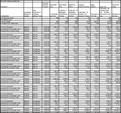
The times in Table 1 are calculated with the following assumptions.
Auto-increment mode - all channels blanked
2byte status + 6 bytes per line (QPLH+QPLL+QPHORIZ) + 6 bytes per four pixels (QPH+QPL+COMMAND)
Individual address mode - all channels blanked
2byte status + 6 bytes per four pixels (QPLH+QPLL+QPHORIZ) + 6 bytes per four pixels (QPH+QPL+COMMAND)
Note: QPLH, QPLL, QPHORIZ, QPH, QPL, COMMAND are internal registers to the MAX4455 related to writing and reading from the SDRAM.
The equations, and the values in the Table 1, do not include the times for checking the status of the RDY/BSY signal, and any computation time required by the processor to prepare data.
The time required when the channels are enabled are calculated by using the above equations and then adding the active video time for each scan line.
The chart in Figure 2, using data from Table 1, graphs the time to perform an update versus the number of pixels that need to written to memory. The plotted data is for the individual address mode with all channels blanked. The three different lines represent three different processor I/O speeds.
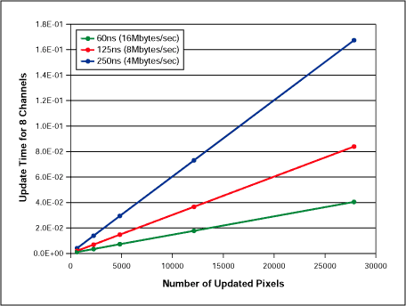
Figure 2. MAX4455 Update time versus number of pixels (individual address mode with all channels blanked).
We will now take a closer look at each of the issues that affects the update rate.
The RDY/BSY signal is initially asserted on power-up even though the MAX4455 is continuously reading from memory. The host writes the address and data values into the QPH, QPL, QPHORIZ, QPLINEH, QPLINEL registers. Once the write bit is set in the command register the MAX4455 checks for availability of the memory interface. If the interface is available the MAX4455 writes the values into memory. If the interface is unavailable the MAX4455 de-asserts the RDY/BSY and then waits to write at the next available time slot. Once it writes the values it then asserts the RDY/BSY signal.
The multi-write function, controlled by the MWRITE command register, can be used in the special case where the exact same graphic is displayed on two or more channels at the same location. The channels that should receive the same data are selected by setting the appropriate bits in the MWRITE register. With these bit(s) set, the MAX4455 automatically writes the same data into the selected channels' corresponding memory locations with a single write command by the host processor. Using the multi-write command will increase the update rate compared to writing each of the channels separately and also reduce the burden on the processor.
The shared memory function, controlled by a group of registers, can also be used in the special case where the same exact data is displayed on more than one channel. By specifying the beginning and ending lines of the portion of one channel that should be shared with as many as three other specified channels the number of pixels that must be updated can be reduced by a factor of four. Even numbered channels can be shared with even numbered channels and odd numbered channels can be shared with odd numbered channels. The limitation of this function is that whole lines must be shared, not individual pixels. In the extremes, it is possible to share information between four unique pairs of channels, or the same information on all eight channels.
In addition to the auto-increment, software can also take advantage of static nature of the register contents on the MAX4455. Data is written into the SDRAM memory by first writing the address and data into register in the MAX4455. Software routines can take advantage of the fact that the data in these registers is static, in that the data in a given register does not change until the user writes new data into that register. If the data does not change for a series of pixels it does not have to be written again until a change in the brightness is desired.
Another improvement can be made when displaying text strings. Take the simple example of a time stamp. If the fonts that represent the numbers are chosen to be a mono-spaced, rather than a proportional font, an individual character can be updated without changing the entire string of text.
Background
The digital portion of a MAX4455-based display system consists of a microcontroller (host processor), SDRAM memory, and the MAX4455, which acts as the interface between the host and the memory. This is illustrated in Figure 1.
Figure 1. MAX4455 key interface signals.
Graphics data to be displayed is contained in the SDRAM memory. The organization of the data for the eight channels is via logical blocks of 512 by 1024 by 4 for each channel for a total of 2Mbits per channel and a total of 16Mbits for all eight channels. The visible pixels on the display map into memory differently for NTSC versus PAL video formats. For NTSC, 484 bits out of the 512 bits in one dimension are used to represent the 484 visible video horizontal scan lines and 712 bits out of 1024 in the other dimension are used to represent the total visible horizontal pixels per line. For the PAL format, all 512 bits are used to represent 512 video horizontal scan lines with the same 712 visible horizontal pixels per line resolution as in NTSC. In both formats, each pixel has a 4-bit resolution to represent brightness.
The interface between the SDRAM memory and the host processor is via the MAX4455. Data intended for the memory is first written into the MAX4455. The MAX4455 in turn, writes this data into the external SDRAM. If the display for the channel is enabled (not blanked), the MAX4455 reads the data from the appropriate location in the external SDRAM, processes the data, and presents the corresponding level for OSDFIL and the associated timing on OSDKEY to drive and control the insertion via the external fast MUX. This memory read sequence operates continuously during the active portion of the video signal. Because the MAX4455 synchronizes to the incoming video, the memory read cycles are inherently asynchronous with respect to the host processor clock.
Data is written and read from the SDRAM by writing an address into the address registers and data into the data registers, then writing to the command register in the MAX4455 to execute the write (or read) to (from) memory. On power-up the MAX4455 automatically writes zero values into all addressable locations in the external memory.
The interface between the host controller and the MAX4455 is a parallel bus consisting of 8 data/address lines (AD0-AD7), with individual control lines for address/data (ADDR/DATA), read (RD), write (WR), chip select (CS), and ready/busy (RDY/BSY).
Optimizing the Graphics Update Rate
The graphics update rate of the MAX4455 is affected by the following:- The size of the graphic.
- The microcontroller I/O speed.
- Use of the BLANK control function.
- Monitoring of the RDY/BSY control line.
- Use of auto-increment, multi-write and shared memory functions.
- The strategy for creating a graphic.

For Larger Image. (PDF, 26KB)
The times in Table 1 are calculated with the following assumptions.
Auto-increment mode - all channels blanked
2byte status + 6 bytes per line (QPLH+QPLL+QPHORIZ) + 6 bytes per four pixels (QPH+QPL+COMMAND)
Individual address mode - all channels blanked
2byte status + 6 bytes per four pixels (QPLH+QPLL+QPHORIZ) + 6 bytes per four pixels (QPH+QPL+COMMAND)
Note: QPLH, QPLL, QPHORIZ, QPH, QPL, COMMAND are internal registers to the MAX4455 related to writing and reading from the SDRAM.
The equations, and the values in the Table 1, do not include the times for checking the status of the RDY/BSY signal, and any computation time required by the processor to prepare data.
The time required when the channels are enabled are calculated by using the above equations and then adding the active video time for each scan line.
The chart in Figure 2, using data from Table 1, graphs the time to perform an update versus the number of pixels that need to written to memory. The plotted data is for the individual address mode with all channels blanked. The three different lines represent three different processor I/O speeds.

Figure 2. MAX4455 Update time versus number of pixels (individual address mode with all channels blanked).
We will now take a closer look at each of the issues that affects the update rate.
Size of the graphic
Obviously, a larger graphic contains more pixels, which means that more data must be written. A simple suggestion is to make the graphic as small as possible to achieve the fastest update rate, i.e. use a smaller font in the case of a text display. Increases in the size of the graphic causes a proportionally larger increase in the number of pixels. For example: a 2X increase in both dimensions of a given graphic causes a 4X increase in the number of pixels.Microcontroller I/O speed
The speed of the microcontroller has a direct effect on the graphics update rate as can be seen from table 1. It is important to note that the critical parameter is the speed of the I/O port that is communicating with the MAX4455 and not the processor clock speed. In many processors it takes more than one clock cycle to write or read from an I/O port.BLANK function
The BLANK function, controlled by one bit in the channel status registers, allows the processor to enable or disable the OSD output on a per channel basis. When an individual channel is disabled (blanked) the OSDFIL and OSDKEY outputs are inactive, but more importantly, the reading of the data for that channel is suspended. This frees up memory access bandwidth to be used by the host processor. The use of the BLANK function can increase the update rate by a factor of about two times. A key tradeoff in the use of the BLANK function is the potential to have flicker on the OSD display. This happens when a channel is blanked for too long of a time. A blanking time of less than a single frame is not noticeable if it occurs on a random basis. Any repetitive blanking may be noticeable and may be viewed as objectionable flicker depending on the repetition rate of the blanking. The exact blanking rate to achieve a smooth display without perceptual flicker depends on a number of system related factors with the most important being human perception. Each system design should be evaluated and optimized for the desired visual performance.Ready/Busy output
The RDY/BSY output of the MAX4455 signals the processor that the MAX4455 is ready to accept another address or data intended for the SDRAM memory. It is important to restate here that this signal is asynchronous with the host processor, and its assertion or de-assertion cannot be predicted. The only reasonable way to use this output is for the host to monitor it continuously, usually via an I/O configured as a processor interrupt.The RDY/BSY signal is initially asserted on power-up even though the MAX4455 is continuously reading from memory. The host writes the address and data values into the QPH, QPL, QPHORIZ, QPLINEH, QPLINEL registers. Once the write bit is set in the command register the MAX4455 checks for availability of the memory interface. If the interface is available the MAX4455 writes the values into memory. If the interface is unavailable the MAX4455 de-asserts the RDY/BSY and then waits to write at the next available time slot. Once it writes the values it then asserts the RDY/BSY signal.
The auto-increment function, multi-write function, and shared memory function
The auto-increment function, controlled by a single bit in the channel status register, is used when sequential locations are written into memory, which represents either horizontal or vertical lines on the display. When the VINC bit in the channel status is set, the vertical address is automatically incremented after each read or write operation. Similarly, when the HINC bit in the channel status register is set; the horizontal address is automatically incremented to the next quad-pixel location after each read or write operation. In this way successive data can be written without having to write the corresponding addresses, thereby increasing the update rate.The multi-write function, controlled by the MWRITE command register, can be used in the special case where the exact same graphic is displayed on two or more channels at the same location. The channels that should receive the same data are selected by setting the appropriate bits in the MWRITE register. With these bit(s) set, the MAX4455 automatically writes the same data into the selected channels' corresponding memory locations with a single write command by the host processor. Using the multi-write command will increase the update rate compared to writing each of the channels separately and also reduce the burden on the processor.
The shared memory function, controlled by a group of registers, can also be used in the special case where the same exact data is displayed on more than one channel. By specifying the beginning and ending lines of the portion of one channel that should be shared with as many as three other specified channels the number of pixels that must be updated can be reduced by a factor of four. Even numbered channels can be shared with even numbered channels and odd numbered channels can be shared with odd numbered channels. The limitation of this function is that whole lines must be shared, not individual pixels. In the extremes, it is possible to share information between four unique pairs of channels, or the same information on all eight channels.
Strategy for changing the graphic
Most graphic images have some amount of spatial redundancy or at least a recurring pattern. By carefully crafting the sequence for drawing the graphic, the total amount of pixels that must be changed at any one time can be reduced. Take the case of a menu with a solid background that occupies the entire screen. It is more efficient to fill the entire background first by taking advantage of the auto-increment function and then individually change the pixels related to the menu items.In addition to the auto-increment, software can also take advantage of static nature of the register contents on the MAX4455. Data is written into the SDRAM memory by first writing the address and data into register in the MAX4455. Software routines can take advantage of the fact that the data in these registers is static, in that the data in a given register does not change until the user writes new data into that register. If the data does not change for a series of pixels it does not have to be written again until a change in the brightness is desired.
Another improvement can be made when displaying text strings. Take the simple example of a time stamp. If the fonts that represent the numbers are chosen to be a mono-spaced, rather than a proportional font, an individual character can be updated without changing the entire string of text.
 电子发烧友App









评论