 电子发烧友App


|
Reference Design for a High-Current Power Supply with Lossless Current Sensing Using the MAX5060 abstract: This reference design shows how to use a MAX5060 current-mode, step-down power-supply controller to implement lossless current sensing for high-current applications. In this design, the series resistance (DCR) of the inductor is used for current sensing to avoid power loss in the current-sense resistor. IntroductionToday's data processing elements demand higher currents from power supplies to achieve higher speed. Lossless current sensing and ground bouncing are key challenges for accurate control of output voltage and current in these applications.The MAX5060 PWM buck power-supply controller uses an average-current-mode control technique to track the load current, and it employs differential sensing to accurately control the output voltage. In this reference design, the series resistance (DCR) of the inductor is used for current sensing to avoid power loss in the current-sense resistor. This design shows a solution for implementing a high-current (30A) power supply with high system efficiency and good load regulation. The complete schematic, bill of materials (BOM), efficiency measurements, and test results are included below. Specifications and Design SetupThis reference design achieves the following specifications.Input Voltage: 12V ±10% Output Voltage: 1.5V Output Current: 30A Output Ripple: ±15mV Input Ripple: ±250mV Efficiency: > 88% with Half of Full Load (15A) Switching Frequency: 275kHz Footprint Size: 5cm × 3.3cm The schematic for this reference design is shown in Figure 1, and the BOM is given in Table 1. In this design, the MAX5060 is used in a buck configuration. 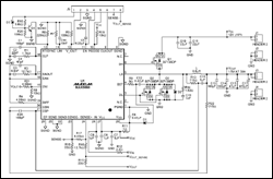 More detailed image (PDF, 100kB) Figure 1. Schematic of the MAX5060 buck converter for FSW = 275kHz. Table 1. Bill of Materials
Efficiency PlotsFigure 2 provides a plot of efficiency versus load current plots for this design, and Figure 3 presents load-regulation data.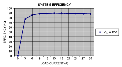 Figure 2. Load current versus converter efficiency for VIN = 12V. 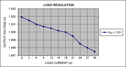 Figure 3. Load current versus converter output voltage for VIN = 12V. Experimental ResultsConverter output voltage and load current are shown in Figures 4–7 for different input excitations.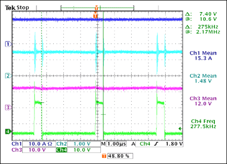 Figure 4. Converter waveforms with VIN = 12V and IOUT = 30A. VIN = 12V and IOUT = 2 × 15A Ch1: Output Current (2x) Ch2: Output Voltage Ch3: Input Voltage Ch4: High-Side MOSFET Gate Drive 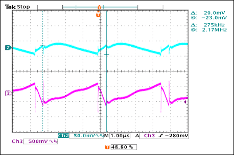 Figure 5. Input and output ripple waveforms with VIN = 12V and IOUT = 30A. VIN = 12V and IOUT = 2 × 15A Ch2: Output Voltage Ripple Ch3: Input Voltage Ripple 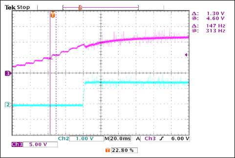 Figure 6. Line transient response. VIN = 0 to 12V and IOUT = 2 × 15A Ch2: Output Voltage Ch3: Input Voltage 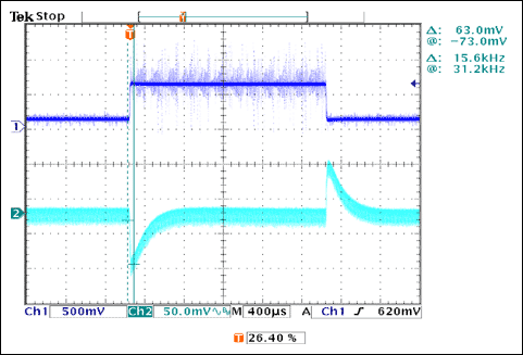 Figure 7. Load transient response. VIN = 12V and IOUT = 1A to 7A Ch1: Output Current Transient (1A to 7A) Ch2: Output Voltage Ripple The board developed for this application is shown in Figure 8. |
Reference Design for a High-Cu
- LO(39007)
- MAX5060(5937)


相关推荐
CU320-2PN RDY一直亮橙色指示灯是什么意思?怎么解决?
大家好,我有一个CU320-2PN 驱动系统带了3个轴,在公司调试的时候是正常的,设备发到现场后发现 RDY一直常亮橙色指示灯,查阅资料显示初始化固件,搞不懂什么意思,是需要升级固件吗?谢谢各位大神1
2024-01-09 14:07:56
请问AD8302的Reference Input可以在A、B两路输入中任意选择吗?
本以为AD8302的Vmag输出和两路输入信号的幅值对数比是一个简单的正比例关系,但看数据手册的图表TPC1、2发现,以不同的输入引脚作为reference input,Vmag相对幅值比的比例系数
2023-12-11 06:18:13
请教如何查看CU320卡里存贮的CU组态数据?
6SL3120-2TE15-0AA3 5A/5A Sinamics S120来驱动。CU320里面的SD卡的文件也能拿到。请问有什么办法能知道电机的具体型号?
2023-11-17 07:09:31
100V同步降压,内置mos,输出电流5A-ZCC1005
400µA operating quiescent current
100V 400-mΩ high-side MOSFET
Peak Current mode control
2023-11-09 15:48:40
读取cu320变频控制器参数时,如何填写参数地址?
请问,通过上位机读取cu320变频控制器参数时,如何填写参数地址? 我们已经通过上位机实现读取cu320数据功能,如读取DB37.DBD1024。但我们不知道cu320中参数地址的映射关系,如我们想
2023-11-06 07:12:37
Cu-Clip互连技术有哪些特点呢?
Cu-Clip技术,它可以应用在很多模块封装形式当中。它的特点有:降低寄生电感和电阻,增加载流能力,相应地提高可靠性,以及灵活的形状设计。
2023-10-07 18:18:28 809
809
809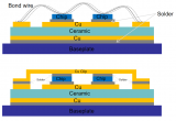

3D Cu-Cu混合键合技术的优点和未来发展
先进半导体封装的凸块技术已取得显着发展,以应对缩小接触间距和传统倒装芯片焊接相关限制带来的挑战。该领域的一项突出进步是 3D Cu-Cu 混合键合技术,它提供了一种变革性的解决方案。
2023-09-21 15:42:29580
580


 工商网监
工商网监
评论