 新一代智能电子化学传感器的新型传感器接口IC ADuCM355详解
ADI公司的ADuCM355是新一代智能电子化学传感器的新型传感器接口IC,能够在单个芯片上同时实现恒电位仪和电化学阻抗频谱分析仪(EIS)功能的唯一解决方案。器件集成了行业最先进的传感器诊断技术,具有卓越的低噪声和低功耗性能,并且尺寸最小,显著节约成本。主要用在工业气体检测,仪器仪表,生命体征监测和疾病管理等。本文介绍了ADuCM355主要特性,功能框图,应用电路以及评估板EVAL-ADuCM355QSPZ主要特性和应用连接图。
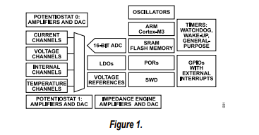
The ADuCM355 is an on-chip system designed to control andmeasure electrochemical and biosensors. The ADuCM355 is an ultralow power mixed-signal microcontroller based on theARMRCortex™-M3 processor. It is designed with current, voltage, and impedance measurement capability. The ADuCM355 features a 16-bit, 400 kSPS multichannel successive approximation register (SAR) analog-to-digitalconverter (ADC) with input buffers, built in antialias filter(AAF) and programmable gain amplifier (PGA)。 The current inputs include three transimpedance amplifiers (TIA) with programmable gain and load resistors for measuring differentsensor types. The analog front end (AFE) also contains twomore low power amplifiers designed specifically for potentiostat capability to maintain a constant bias voltage to an external electrochemical sensor. The noninverting inputs of these twoamplifiers are controlled by on-chip dual output digital-to-analog converters (DAC)。 The analog outputs include anotherhigh speed DAC and output amplifier designed to generate an ac signal. The ADC is capable of operating at conversion rates up to 400 kSPS with an input range of ±0.9 V. An input mux before the ADC allows the user to select an input channel formeasurement. These input channels include three externalcurrent inputs, multiple external voltage inputs, and internal channels. The internal channels allow diagnostic measurementsof the internal supply voltages, die temperature, and referencevoltages. Two of the three voltage DACs are dual output, 12-bit stringDACs. One output per DAC controls the noninverting input of a potentiostat amplifier, and the other controls the noninverting input of the TIA.
The third DAC (sometimes referred to as the high speed DAC)is designed for the high power TIA for impedancemeasurements. Its output frequency range is up to 200 kHz. A precision 1.82 V and 2.5 V on-chip reference source is available. The internal ADC and VDAC circuits use this on-chip reference source to ensure low drift performance for all of these peripherals.
The ADuCM355 integrates a 26 MHz ARM Cortex-M3processor. It is a 32-bit reduced instruction set computer (RISC) machine, offering up to 32.5 DMIPS peak performance. The ARM Cortex-M3 processor also has a flexible multichannel direct memory access controller (DMA) supporting serial peripheral interface (two independent SPI ports), universalasynchronous receiver/transmitter (UART), and I2Ccommunication peripherals. The ADuCM355 has 128 kB of nonvolatile flash/EE memory and 64 kB of SRAM integrated on-chip. The digital processor subsystem is clocked from a 26 MHz on-chip oscillator. This is the source of the main digital die systemclock. Optionally, a 26 MHz PLL can be used as the digitalsystem clock. This clock can be internally subdivided so that the processor operates at a lower frequency and saves power. A lowpower internal 32 kHz oscillator is available and can clock thetimers. The ADuCM355 includes three general-purpose timers,a wake-up timer (which can be used as a general-purposetimer), and a system watchdog timer. The analog subsystem has a separate 16 MHz oscillator used to clock the ADC, DACs, and other digital logic on the analog die.
The analog die also contains a separate 32 kHz, low poweroscillator to clock a watchdog timer on the low voltage die. Both the 32 kHz oscillator and this watchdog are independent from the digital die oscillators and system watchdog timer. A range of communication peripherals can be configured asrequired in a specific application. These peripherals includeUART, I2C, 2xSPI, and GPIO ports. The GPIO, combined with the general-purpose timers, can be combined to generate apulse width modulation (PWM) type output. On-chip factory firmware supports in-circuit erasing of user flashtriggered via the UART, while nonintrusive emulation and programdownload are supported via the serial wire debug port (SW-DP) interface. The ADuCM355 operates from 2.8 V to 3.6 V supply and isspecified over a temperature range of −40℃ to +85℃。 The chip is packaged in a 72-lead 6 mm × 5 mm land grid array (LGA)package.
ADuCM355主要特性:
Analog input/output
16-bit, 400 kSPS ADC
Voltage, current, and impedance measurement capability
Internal/external current and voltage channels
Ultralow leakage switch matrix and input mux
Input buffers, programmable gain amplifier
Voltage DACs
2 dual output VDACs Output range 0.2 V to 2.4 V (±2.2 V voltage potential to sensor)
2 bias potentiostat and TIA amplifiers
Ultralow power, 1 μA per DAC
One high speed 12-bit VDAC
Output range to sensor ±607 mV
High speed TIA for impedance measurements
Programmable gain amplifier on output
Amplifiers, accelerators, and references 2 low power, low noise amplifiers
Suitable for potentiostat bias in electrochemical sensing
2 low power, low noise TIAs Suitable for measuring sensor current output 200 pA to 3 mA range Programmable load and gain resistors Analog hardware accelerators DDS waveform generator
DFT and digital filters 2.5 V and 1.82 V on-chip, precision voltage references Internal temperature sensor, ±2℃ accurate
Impedance measurement range of 《1 Ω to 10 MΩ, 1 Hz to 200 kHz
Voltammetry scan rate up to 2000 steps per second
Microcontroller
26 MHz ARM Cortex-M3 processor
Serial wire port supports code download and debug
128 kB flash/64 kB of SRAM
Security/safety
Hardware crypto accelerator with AES-128 and AES-256
Hardware CRC with programmable polynomial generator Read/write protection of user flash
On-chip peripherals
UART, I2C, and SPI serial input/output
Up to 10 GPIO pins
External interrupt option
General-purpose, wake-up, and watchdog timers
Power
2.8 V to 3.6 V supply and active measurement range
Power-supply monitor
Active current consumption 30 μA/MHz for digital part
Hibernate with bias to external sensor, 8.5 μA
Shutdown mode with no SRAM retention, 2 μA
Packages and temperature range
6 mm × 5 mm, 72-lead LGA package
Fully specified for −40℃ to +85℃ ambient operation
ADuCM355应用:
Gas detection Food quality
Environmental sensing (air, water, soil)
Blood glucose meters
Life sciences and biosensing analysis
Bioimpedance measurements
General Amperometry, voltammetry, and impedance
spectroscopy functions

图1.ADuCM355简化功能框图

图2.ADuCM355功能框图

图3.ADuCM355推荐的外接元件连接图
评估板EVAL-ADuCM355QSPZ
The ADuCM355 system on a chip provides the features needed to bias and measure a range of different electrochemical sensors. The EVAL-ADuCM355QSPZ allows users to evaluate the performance of the ADuCM355 when implementing a range of different electrochemical techniques, including chronoam-perometry, voltammetry, and electrochemical impedance spectroscopy (EIS)。
评估板EVAL-ADuCM355QSPZ主要特性:
Debug/programming capability of ADuCM355
Evaluation capability with electrochemical gas sensors
ADT7420 0.5 C accurate temperature sensor via I2C
USB power option and connection to PC
图4.评估板EVAL-ADuCM355QSPZ外形图

图5.JP45和JP46连接ADuCM355 UART引脚到USB收发器


图7.HSTIA可编增益电阻
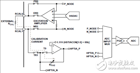
图8.用来RTIA2校准的HSDAC HSTIA和开关矩阵设定图

图9.用于RTIA2_03校准的HSDAC HSTIA和开关矩阵设定图

图10.用于RTIA2_05校准的HSDAC HSTIA和开关矩阵设定图
-
传感器
+关注
关注
2561文章
52318浏览量
762404 -
ti
+关注
关注
113文章
8015浏览量
214182
发布评论请先 登录
开发新型传感器的途径
开发新型传感器的途径
浅析化学传感器和纳米传感器
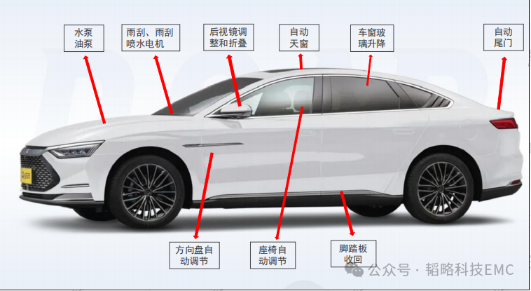
基于微型传感器的汽车电子化智能化工程应用
新一代磁性位置传感器助力无人机、轻工业、医疗以及太空机器人应用有哪些?
ADUCM355 具有化学传感器接口的精密模拟微控制器

ADuCM355和LTC6078解决方案
ADUCM356集成化学传感器接口的精密模拟微控制器技术手册

瑞萨RA8系列教程 | 基于 RASC 生成 Keil 工程
对于不习惯用 e2 studio 进行开发的同学,可以借助 RASC 生成 Keil 工程,然后在 Keil 环境下愉快的完成开发任务。

共赴之约 | 第二十七届中国北京国际科技产业博览会圆满落幕
作为第二十七届北京科博会的参展方,芯佰微有幸与800余家全球科技同仁共赴「科技引领创享未来」之约!文章来源:北京贸促5月11日下午,第二十七届中国北京国际科技产业博览会圆满落幕。本届北京科博会主题为“科技引领创享未来”,由北京市人民政府主办,北京市贸促会,北京市科委、中关村管委会,北京市经济和信息化局,北京市知识产权局和北辰集团共同承办。5万平方米的展览云集

道生物联与巍泰技术联合发布 RTK 无线定位系统:TurMass™ 技术与厘米级高精度定位的深度融合
道生物联与巍泰技术联合推出全新一代 RTK 无线定位系统——WTS-100(V3.0 RTK)。该系统以巍泰技术自主研发的 RTK(实时动态载波相位差分)高精度定位技术为核心,深度融合道生物联国产新兴窄带高并发 TurMass™ 无线通信技术,为室外大规模定位场景提供厘米级高精度、广覆盖、高并发、低功耗、低成本的一站式解决方案,助力行业智能化升级。

智能家居中的清凉“智”选,310V无刷吊扇驱动方案--其利天下
炎炎夏日,如何营造出清凉、舒适且节能的室内环境成为了大众关注的焦点。吊扇作为一种经典的家用电器,以其大风量、长寿命、低能耗等优势,依然是众多家庭的首选。而随着智能控制技术与无刷电机技术的不断进步,吊扇正朝着智能化、高效化、低噪化的方向发展。那么接下来小编将结合目前市面上的指标,详细为大家讲解其利天下有限公司推出的无刷吊扇驱动方案。▲其利天下无刷吊扇驱动方案一
电源入口处防反接电路-汽车电子硬件电路设计
一、为什么要设计防反接电路电源入口处接线及线束制作一般人为操作,有正极和负极接反的可能性,可能会损坏电源和负载电路;汽车电子产品电性能测试标准ISO16750-2的4.7节包含了电压极性反接测试,汽车电子产品须通过该项测试。二、防反接电路设计1.基础版:二极管串联二极管是最简单的防反接电路,因为电源有电源路径(即正极)和返回路径(即负极,GND),那么用二极

半导体芯片需要做哪些测试
首先我们需要了解芯片制造环节做⼀款芯片最基本的环节是设计->流片->封装->测试,芯片成本构成⼀般为人力成本20%,流片40%,封装35%,测试5%(对于先进工艺,流片成本可能超过60%)。测试其实是芯片各个环节中最“便宜”的一步,在这个每家公司都喊着“CostDown”的激烈市场中,人力成本逐年攀升,晶圆厂和封装厂都在乙方市场中“叱咤风云”,唯独只有测试显

解决方案 | 芯佰微赋能示波器:高速ADC、USB控制器和RS232芯片——高性能示波器的秘密武器!
示波器解决方案总述:示波器是电子技术领域中不可或缺的精密测量仪器,通过直观的波形显示,将电信号随时间的变化转化为可视化图形,使复杂的电子现象变得清晰易懂。无论是在科研探索、工业检测还是通信领域,示波器都发挥着不可替代的作用,帮助工程师和技术人员深入剖析电信号的细节,精准定位问题所在,为创新与发展提供坚实的技术支撑。一、技术瓶颈亟待突破性能指标受限:受模拟前端
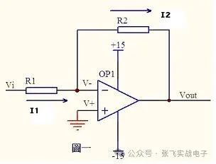
硬件设计基础----运算放大器
1什么是运算放大器运算放大器(运放)用于调节和放大模拟信号,运放是一个内含多级放大电路的集成器件,如图所示:左图为同相位,Vn端接地或稳定的电平,Vp端电平上升,则输出端Vo电平上升,Vp端电平下降,则输出端Vo电平下降;右图为反相位,Vp端接地或稳定的电平,Vn端电平上升,则输出端Vo电平下降,Vn端电平下降,则输出端Vo电平上升2运算放大器的性质理想运算

ElfBoard技术贴|如何调整eMMC存储分区
ELF 2开发板基于瑞芯微RK3588高性能处理器设计,拥有四核ARM Cortex-A76与四核ARM Cortex-A55的CPU架构,主频高达2.4GHz,内置6TOPS算力的NPU,这一设计让它能够轻松驾驭多种深度学习框架,高效处理各类复杂的AI任务。
米尔基于MYD-YG2LX系统启动时间优化应用笔记
1.概述MYD-YG2LX采用瑞萨RZ/G2L作为核心处理器,该处理器搭载双核Cortex-A55@1.2GHz+Cortex-M33@200MHz处理器,其内部集成高性能3D加速引擎Mail-G31GPU(500MHz)和视频处理单元(支持H.264硬件编解码),16位的DDR4-1600/DDR3L-1333内存控制器、千兆以太网控制器、USB、CAN、
运放技术——基本电路分析
虚短和虚断的概念由于运放的电压放大倍数很大,一般通用型运算放大器的开环电压放大倍数都在80dB以上。而运放的输出电压是有限的,一般在10V~14V。因此运放的差模输入电压不足1mV,两输入端近似等电位,相当于“短路”。开环电压放大倍数越大,两输入端的电位越接近相等。“虚短”是指在分析运算放大器处于线性状态时,可把两输入端视为等电位,这一特性称为虚假短路,简称
飞凌嵌入式携手中移物联,谱写全国产化方案新生态
4月22日,飞凌嵌入式“2025嵌入式及边缘AI技术论坛”在深圳成功举办。中移物联网有限公司(以下简称“中移物联”)携OneOS操作系统与飞凌嵌入式共同推出的工业级核心板亮相会议展区,操作系统产品部高级专家严镭受邀作《OneOS工业操作系统——助力国产化智能制造》主题演讲。
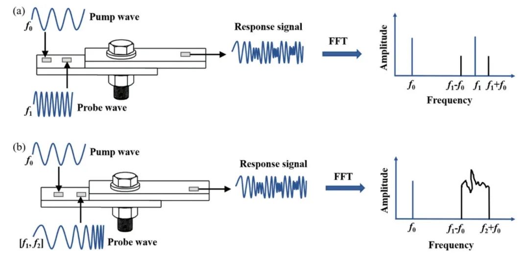
ATA-2022B高压放大器在螺栓松动检测中的应用
实验名称:ATA-2022B高压放大器在螺栓松动检测中的应用实验方向:超声检测实验设备:ATA-2022B高压放大器、函数信号发生器,压电陶瓷片,数据采集卡,示波器,PC等实验内容:本研究基于振动声调制的螺栓松动检测方法,其中低频泵浦波采用单频信号,而高频探测波采用扫频信号,利用泵浦波和探测波在接触面的振动声调制响应对螺栓的松动程度进行检测。通过螺栓松动检测
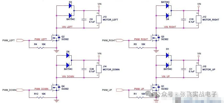
MOS管驱动电路——电机干扰与防护处理
此电路分主电路(完成功能)和保护功能电路。MOS管驱动相关知识:1、跟双极性晶体管相比,一般认为使MOS管导通不需要电流,只要GS电压(Vbe类似)高于一定的值,就可以了。MOS管和晶体管向比较c,b,e—–>d(漏),g(栅),s(源)。2、NMOS的特性,Vgs大于一定的值就会导通,适合用于源极接地时的情况(低端驱动),只要栅极电压达到4V或10V就可以
压敏(MOV)在电机上的应用剖析
一前言有刷直流电机是一种较为常见的直流电机。它的主要特点包括:1.结构相对简单,由定子、转子、电刷和换向器等组成;2.通过电刷与换向器的接触来实现电流的换向,从而使电枢绕组中的电流方向周期性改变,保证电机持续运转;3.具有调速性能较好等优点,可以通过改变电压等方式较为方便地调节转速。有刷直流电机在许多领域都有应用,比如一些电动工具、玩具、小型机械等。但它也存


 工商网监
工商网监
评论